The LRU bits are initialized to 000000 by a power-on reset, but are not initialized by a manual
reset.
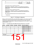
Table 5.2 LRU and Way Replacement (When the cache lock function is not used)
LRU (5–0)
Way to be Replaced
000000, 000100, 010100, 100000, 110000, 110100
000001, 000011, 001011, 100001, 101001, 101011
000110, 000111, 001111, 010110, 011110, 011111
111000, 111001, 111011, 111100, 111110, 111111
3
2
1
0
5.1.3
Register Configuration
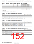
Table 5.3 shows details of the cache control register.
Table 5.3 Register Configuration
Register
Abbr.
CCR
R/W
R/W
R/W
Initial Value
Address
Access Size
Cache control register
Cache control register 2
H'00000000
H'00000000
H'FFFFFFEC 32-bit
CCR2
H'040000B0
(H’A40000B0)
32-bit
*
Note: * When address translation by the MMU does not apply, the address in parentheses should
be used.
5.2
Register Description
5.2.1
Cache Control Register (CCR)
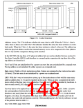
The cache is enabled or disabled using the CE bit of the cache control register (CCR). CCR also
has a CF bit (which invalidates all cache entries), and a WT and CB bits (which select either write-
through mode or write-back mode). Programs that change the contents of the CCR register should
be placed in address space that is not cached. When updating the contents of the CCR register,
always set bits 4 to 0. Figure 5.2 shows the configuration of the CCR register.
Rev. 5.00, 09/03, page 105 of 760

 RENESAS [ RENESAS TECHNOLOGY CORP ]