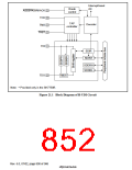
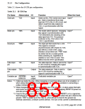
21.1.3 Pin Configuration
Table 21.1 shows the H-UDI pin configuration.
Table 21.1 H-UDI Pins
Pin Name
Abbreviation I/O
Function
When Not Used
1
*
Clock pin
TCK
Input
Same as the JTAG serial clock input Open
pin. Data is transferred from data
input pin TDI to the H-UDI circuit, and
data is read from data output pin
TDO, in synchronization with this
signal.
1
*
Mode pin
Reset pin
TMS
7567
Input
Input
The mode select input pin. Changing Open
this signal in synchronization with
TCK determines the meaning of the
data input from TDI. The protocol
conforms to the JTAG (IEEE Std
1149.1) specification.
*2 *3
The input pin that resets the H-UDI.
This signal is received
asynchronously with respect to TCK,
and effects a reset of the JTAG
interface circuit when low. 7567 must
be driven low for a certain period
when powering on, regardless of
whether or not JTAG is used. This
differs from the IEEE specification.
1
*
*
Data input
pin
TDI
Input
The data input pin. Data is sent to the Open
H-UDI circuit by changing this signal
in synchronization with TCK.
Data output TDO
pin
Output The data output pin. Data is sent to
Open
the H-UDI circuit by reading this
signal in synchronization with TCK.
1
Emulator pin $6(%5./
Input/
output
Dedicated emulator pin
Open
BRKACK
Notes: *1 Pulled up inside the chip. When designing a board that allows use of an emulator, or
when using interrupts and resets via the H-UDI, there is no problem in connecting a
pullup resistance externally.
*2 When designing a board that enables the use of an emulator, or when using interrupts
and resets via the H-UDI, drive 7567 low for a period overlapping 5(6(7 at power-on,
and also provide for control by 7567 alone.
*3 Fixed to the ground or connected to the same signal line as 5(6(7/#or to a signal line
that behaves in the same way. However, there is a problem when this pin is fixed to the
ground. 7567 is pulled up in the chip so, when this pin is fixed to the ground via
external connection, a minute current will flow. The size of this current is determined by
Rev. 6.0, 07/02, page 801 of 986

 RENESAS [ RENESAS TECHNOLOGY CORP ]