Section 21 Hitachi User Debug Interface (H-UDI)
21.1
Overview
21.1.1 Features
The Hitachi user debug interface (H-UDI) is a serial input/output interface conforming to JTAG,
IEEE 1149.1, and IEEE Standard Test Access Port and Boundary-Scan Architecture. The
SH7750R’s H-UDI supports boundary-scan, but is used for emulator connection as well. The
functions of this interface should not be used when using an emulator. Refer to the emulator
manual for the method of connecting the emulator. The H-UDI uses six pins (TCK, TMS, TDI,
TDO, 7567, and $6(%5./BRKACK). The pin functions and serial transfer protocol conform to
the JTAG specifications.
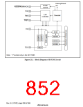
21.1.2 Block Diagram
Figure 21.1 shows a block diagram of the H-UDI. The TAP (test access port) controller and
control registers are reset independently of the chip reset pin by driving the 7567 pin low or
setting TMS to 1 and applying TCK for at least five clock cycles. The other circuits are reset and
initialized in an ordinary reset. The H-UDI circuit has four internal registers: SDBPR, SDIR,
SDDRH, and SDDRL (these last two together designated SDDR). The SDBPR register supports
the JTAG bypass mode, SDIR is the command register, and SDDR is the data register. SDIR can
be accessed directly from the TDI and TDO pins.
Rev. 6.0, 07/02, page 799 of 986

 RENESAS [ RENESAS TECHNOLOGY CORP ]