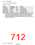
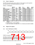
16.1.4 Register Configuration
The SCIF has the internal registers shown in table 16.2. These registers are used to specify the
data format and bit rate, and to perform transmitter/receiver control.
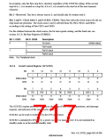
Table 16.2 SCIF Registers
Abbrevia-
tion
Initial
Value
P4
Address
Area 7
Address
Access
Size
Name
R/W
Serial mode register
Bit rate register
Serial control register
SCSMR2 R/W
H'0000
H'FF
H'FFE80000 H'IFE80000 16
H'FFE80004 H'IFE80004 8
H'FFE80008 H'IFE80008 16
SCBRR2
SCSCR2
R/W
R/W
W
H'0000
Transmit FIFO data register SCFTDR2
Serial status register SCFSR2
Receive FIFO data register SCFRDR2 R
Undefined H'FFE8000C H'IFE8000C 8
H'0060 H'FFE80010 H'IFE80010 16
Undefined H'FFE80014 H'IFE80014 8
1
*
R/(W)
FIFO control register
FIFO data count register
Serial port register
SCFCR2
SCFDR2
R/W
R
H'0000
H'0000
H'0000
H'0000
H'FFE80018 H'IFE80018 16
H'FFE8001C H'IFE8001C 16
H'FFE80020 H'IFE80020 16
H'FFE80024 H'IFE80024 16
2
*
SCSPTR2 R/W
3
*
R/(W)
Line status register
SCLSR2
Notes: *1 Only 0 can be written, to clear flags. Bits 15 to 8, 3, and 2 are read-only, and cannot be
modified.
*2 The value of bits 6, 4, and 0 is undefined.
*3 Only 0 can be written, to clear flags. Bits 15 to 1 are read-only, and cannot be modified.
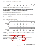
16.2
Register Descriptions
16.2.1 Receive Shift Register (SCRSR2)
Bit:
7
6
5
4
3
2
1
0
R/W:
—
—
—
—
—
—
—
—
SCRSR2 is the register used to receive serial data.
The SCIF sets serial data input from the RxD2 pin in SCRSR2 in the order received, starting with
the LSB (bit 0), and converts it to parallel data. When one byte of data has been received, it is
transferred to the receive FIFO register, SCFRDR2, automatically.
SCRSR2 cannot be directly read or written to by the CPU.
Rev. 6.0, 07/02, page 661 of 986

 RENESAS [ RENESAS TECHNOLOGY CORP ]