15.1.3 Pin Configuration
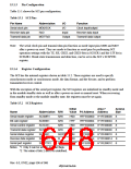
Table 15.1 shows the SCI pin configuration.
Table 15.1 SCI Pins
Pin Name
Abbreviation
MD0/SCK
RxD
I/O
Function
Serial clock pin
Receive data pin
Transmit data pin
I/O
Clock input/output
Receive data input
Transmit data output
Input
Output
MD7/TxD
Note: The serial clock pin and transmit data pin function as mode input pins MD0 and MD7
after a power-on reset. They are made to function as serial pins by performing SCI
operation settings with the TE, RE, CKEI, and CKE0 bits in SCSCR1 and the C/$ bit in
SCSMR1. Break state transmission and detection, can be set in the SCI’s SCSPTR1
register.
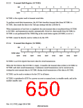
15.1.4 Register Configuration
The SCI has the internal registers shown in table 15.2. These registers are used to specify
asynchronous mode or synchronous mode, the data format, and the bit rate, and to perform
transmitter/receiver control.
With the exception of the serial port register, the SCI registers are initialized in standby mode and
in the module standby state as well as after a power-on reset or manual reset. When recovering
from standby mode or the module standby state, the registers must be set again.
Table 15.2 SCI Registers
Initial
Area 7
Access
Size
Name
Abbreviation R/W
Value P4 Address Address
Serial mode register
Bit rate register
Serial control register
SCSMR1
SCBRR1
SCSCR1
R/W
R/W
R/W
R/W
H'00
H'FF
H'00
H'FF
H'84
H'00
H'FFE00000 H'1FE00000
H'FFE00004 H'1FE00004
H'FFE00008 H'1FE00008
H'FFE0000C H'1FE0000C
H'FFE00010 H'1FE00010
H'FFE00014 H'1FE00014
H'FFE0001C H'1FE0001C
8
8
8
8
8
8
8
Transmit data register SCTDR1
1
*
Serial status register
Receive data register
Serial port register
SCSSR1
SCRDR1
SCSPTR1
R/(W)
R
2
*
H'00
R/W
Notes: *1 Only 0 can be written, to clear flags.
*2 The value of bits 2 and 0 is undefined.
Rev. 6.0, 07/02, page 596 of 986

 RENESAS [ RENESAS TECHNOLOGY CORP ]