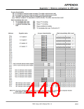
APPENDIX
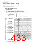
Appendix 1. Memory assigment in SFR area
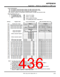
Access characteristics
: It is possible to read the bit state at reading. The written value becomes valid.
: It is possible to read the bit state at reading. The written value becomes invalid.
: The written value becomes valid. It is impossible to read the bit state.
RW
RO
WO
: Nothing is assigned. It is impossible to read the bit state. The written value becomes invalid.
State immediately after reset
: “0” immediately after reset.
: “1” immediately after reset.
: Undefined immediately after
reset.
0
1
?
: Always “0” at reading.
0
1
?
0
: Always “1” at reading.
: Always undefined at reading.
: “0” immediately after reset. Fix this bit to “0.”
Register name
Address
Access characteristics
State immediately after reset
b7
b0
b7
b0
(Note 7)
? (Note 8)
Watchdog timer register
6016
6116
6216
6316
6416
6516
6616
6716
6816
6916
6A16
6B16
6C16
6D16
6E16
6F16
7016
7116
7216
7316
7416
7516
7616
7716
7816
Watchdog timer frequency select register
Particular function select register 0
0
0
0
0
0
0
?
0
RW RW
RW
RW
RW (Note 9)
RW
RW RW RW
0
0
0
0
0
0
0
0
0
0
Particular function select register 1
Particular function select register 2
(Note 10)
(Note 11)
?
?
(Note 12)
(Note 11)
(Note 11)
RW
0
0
0
?
0
0
1
0
Debug control register 0
Debug control register 1
0
0
RO RO
RW RW RO RW
0
0
RW (Note 13)
?
?
Address comparison register 0
RW (Note 13)
RW (Note 13)
RW (Note 13)
RW (Note 13)
RW (Note 13)
RW
?
?
?
?
Address comparison register 1
0
0
0
0
INT3 interrupt control register
INT4 interrupt control register
?
?
0
0
0
0
0
0
0
0
0
0
0
0
0
0
0
0
0
0
0
0
RW
?
A-D conversion interrupt control register
UART0 transmit interrupt control register
UART0 receive interrupt control register
UART1 transmit interrupt control register
UART1 receive interrupt control register
Timer A0 interrupt control register
Timer A1 interrupt control register
Timer A2 interrupt control register
Timer A3 interrupt control register
?
RW
0
0
0
RW
RW
RW
RW
RW
RW
RW
RW
RW
RW
RW
RW
?
?
?
?
?
?
0
0
0
0
0
0
0
0
0
0
0
0
0
0
0
0
0
0
0
0
0
0
0
0
0
0
0
0
0
0
0
0
0
0
0
0
0
0
0
0
0
0
0
0
0
0
0
0
?
?
?
?
?
?
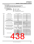
7916 Timer A4 interrupt control register
7A16
7B16
7C16
7D16
7E16
7F16
Timer B0 interrupt control register
Timer B1 interrupt control register
Timer B2 interrupt control register
INT0 interrupt control register
0
0
0
0
0
0
?
?
?
RW
RW
RW
INT1 interrupt control register
INT2 interrupt control register
Notes 7 : By writing dummy data to address 6016, a value of “FFF16” is set to the watchdog timer.
The dummy data is not retained anywhere.
8 : A value of “FFF16” is set to the watchdog timer. (Refer to “CHAPTER 14. WATCHDOG TIMER.”)
9 : After writing “5516” to address 6216, each bit must be set.
10 : It is possible to read the bit state at reading. By writing “0” to this bit, this bit becomes “0.”
But when writing “1” to this bit, this bit will not change.
11 : This bit becomes “0” at power-on reset. This bit retains the state immediately before reset in the case of
hardware reset and software reset.
12 : Do not write to this register.
13 : When these registers are accessed, set the address comparison register access enable bit (bit 2 at address
6716) to “1.” (Refer to “CHAPTER 17. DEBUG FUNCTION.”)
7905 Group User’s Manual Rev.1.0
20-5

 RENESAS [ RENESAS TECHNOLOGY CORP ]