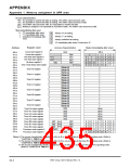
APPENDIX
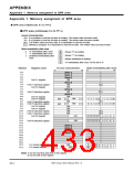
Appendix 1. Memory assigment in SFR area
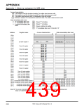
Access characteristics
: It is possible to read the bit state at reading. The written value becomes valid.
: It is possible to read the bit state at reading. The written value becomes invalid.
: The written value becomes valid. It is impossible to read the bit state.
RW
RO
WO
: Nothing is assigned. It is impossible to read the bit state. The written value becomes invalid.
State immediately after reset
: “0” immediately after reset.
: “1” immediately after reset.
: Undefined immediately after
reset.
0
1
?
: Always “0” at reading.
0
1
?
0
: Always “1” at reading.
: Always undefined at reading.
: “0” immediately after reset. Fix this bit to “0.”
Register name
Address
Access characteristics
State immediately after reset
b7
b0
b7
b0
Count start register 0
0016
RW
RW
WO
WO
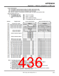
4016
4116
4216
4316
4416
4516
4616
4716
4816
4916
4A16
4B16
4C16
4D16
4E16
4F16
5016
5116
5216
5316
5416
5516
5616
5716
5816
5916
5A16
5B16
5C16
5D16
5E16
5F16
Count start register 1
One-shot start register 0
One-shot start register 1
0
0
0
0
0
0
?
0
0
0
0
0
0
RW
RW
0
?
?
0
0
0
0
0
0
0
0
0
0
0
0
0
0
0
0
Up-down register 0
RW
WO
0
0
0
0
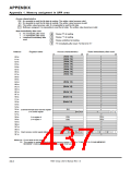
Timer A clock division select register
RW
RW
(Note 4)
(Note 4)
(Note 4)
(Note 4)
(Note 4)
(Note 4)
(Note 4)
(Note 4)
(Note 4)
(Note 4)
(Note 5)
(Note 5)
(Note 5)
(Note 5)
(Note 5)
(Note 5)
RW
?
?
Timer A0 register
Timer A1 register
Timer A2 register
Timer A3 register
Timer A4 register
Timer B0 register
?
?
?
?
?
?
?
?
?
?
?
?
?
Timer B1 register
Timer B2 register
?
Timer A0 mode register
Timer A1 mode register
Timer A2 mode register
Timer A3 mode register
Timer A4 mode register
Timer B0 mode register
Timer B1 mode register
Timer B2 mode register
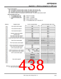
Processor mode register 0
Processor mode register 1
0016
0016
0016
0016
0016
0
RW
RW
RW
RW
(Note 6)
RW
RW
0
0
0
0
0
0
0
0
0
0
?
0
0
0
0
0
0
0
0
0
0
0
0
0
0
1
0
(Note 6)
(Note 6)
0
0
0
0
RW
RW
RW WO
RW
RW
?
?
0
0
0
1
RW
RW
0
0
Notes 4: The access characteristics at addresses 4616 to 4F16 vary according to the timer A’s operating mode. (Refer to
“CHAPTER 7. TIMER A.”)
5: The access characteristics at addresses 5016 to 5516 vary according to the timer B’s operating mode. (Refer to
“CHAPTER 8. TIMER B.”)
6: The access characteristics for bit 5 at addresses 5B16 to 5D16 vary according to the timer B’s operating mode.
(Refer to “CHAPTER 8. TIMER B.”)
7905 Group User’s Manual Rev.1.0
20-4

 RENESAS [ RENESAS TECHNOLOGY CORP ]