A-D CONVERTER
12.2 Block description
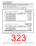
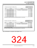
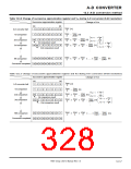
b7 b6 b5 b4 b3 b2 b1 b0
Comparator result register 0 (Address DE16
)
Bit
0
Bit name
Function
At reset R/W
0 : The set value > The input level at pin AN
1 : The set value < The input level at pin AN
i
i
AN
AN
AN
AN
AN
AN
AN
AN
0
1
2
3
4
5
6
7
pin comparator result bit
pin comparator result bit
pin comparator result bit
pin comparator result bit
pin comparator result bit
pin comparator result bit
pin comparator result bit
pin comparator result bit
0
0
0
0
0
0
0
0
RW
RW
RW
RW
RW
RW
RW
RW
1
2
3
4
5
6
7
Note: Writing to comparator result register 0 must be performed while the A-D converter halts.
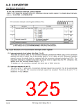
b7 b6 b5 b4 b3 b2 b1 b0
Comparator result register 1 (Address DF16
)
0 0 0 0
Bit
0
Bit name
Function
At reset R/W
0 : The set value > The input level at pin AN
1 : The set value < The input level at pin AN
i
i
AN
8
9
pin comparator result bit
pin comparator result bit
0
0
0
0
0
RW
RW
RW
RW
RW
1
AN
2
AN10 pin comparator result bit
AN11 pin comparator result bit
3
7 to 4 Fix these bits to “0000.”
Note: Writing to comparator result register 1 must be performed while the A-D converter halts.
Fig. 12.2.8 Structures of comparator result register 0 and 1
7905 Group User’s Manual Rev.1.0
12-13

 RENESAS [ RENESAS TECHNOLOGY CORP ]