A-D CONVERTER
12.2 Block description
12.2.5 Port P7 direction register, port P8 direction register
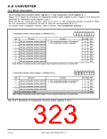
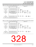
The A-D converter’s input pins are multiplexed with the port P7 and P8 pins. When using these pins as
A-D converter’s input pins, be sure to clear the port P7, P8 direction registers’ bits, corresponding to the
A-D converter’s input pins, in order to set these pins to the input mode. Figure 12.2.10 shows the correspondence
between the port P7, P8 direction registers and the A-D converter’s input pins.
b7 b6 b5 b4 b3 b2 b1 b0
Port P7 direction register (Address 1116)
Bit
0
Bit name
Function
At reset R/W
Pin AN
Pin AN
Pin AN
Pin AN
Pin AN
0
1
2
3
4
0 : Input mode
1 : Output mode
0
0
0
0
0
0
0
0
RW
RW
RW
RW
RW
RW
RW
RW
1
When using any of these pins as A-D converter’s
input pin, be sure to clear its corresponding bit to
“0.”
2
3
4
5
Pin AN5
Pin AN6
6
7
Pin AN7 (Pin DA0)
(Note 1)
Notes 1: When using pin AN
7
, be sure to clear the D-A output enable bit (bit 0 at address 9616) = “0” (output disabled).
0
2: The pins in ( ) is I/O pins of other internal peripheral devices, which are multiplexed with the corresponding port
P7 pin.
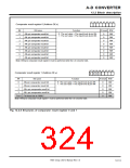
b7 b6 b5 b4 b3 b2 b1 b0
Port P8 direction register (Address 1416)
Bit
0
Bit name
Function
At reset R/W
0 : Input mode
1 : Output mode
Pin AN
8
(Pin CTS2/RTS
2/DA
1
) (Note 1)
0
0
0
RW
RW
1
Pin AN9 (Pin CTS2/CLK2)(Note 2)
When using any of these pins as A-D converter’s input
pin, be sure to clear its corresponding bit to “0.”
2
Pin AN10 (Pin RXD2)
Pin AN11 (Pin TXD2)
(Note 3)
(Note 4)
RW
RW
–
3
0
7 to 5 Nothing is assigned.
Undefined
Notes 1: When using pin AN be sure to clear the D-A
8
1
output enable bit (bit 1 at address 9616) = “0” (output disabled). Also, be sure
not to use pin CTS /RTS
2: When using pin AN , be sure not to use pin CTS
3: When using pin AN10, be sure not to use pin R
4: When using pin AN11, be sure not to use pin T D .
2
2
.
9
2
/CLK .
2
X
D .
2
X
2
5: The pins in ( ) are I/O pins of other internal peripheral devices, which are multiplexed with the corresponding port
P8 pins.
Fig. 12.2.10 Correspondence between port P7, P8 derection registers and A-D converter’s input pins
7905 Group User’s Manual Rev.1.0
12-15

 RENESAS [ RENESAS TECHNOLOGY CORP ]