SERIAL I/O
11.3 Clock synchronous serial I/O mode
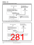
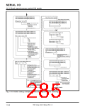
UART0 transmit/receive mode register (Address 3016
UART1 transmit/receive mode register (Address 3816
)
)
When external clock is selected.
UART2 transmit/receive mode register (Address B016
)
When internal clock is selected.
b7
b0
UART0 baud rate register (BRG0) (Address 3116
UART1 baud rate register (BRG1) (Address 3916
)
)
0 ꢀ ꢀ ꢀ
0
0
1
Selection of clock synchronous serial
I/O mode
UART2 baud rate register (BRG2) (Address B116
)
b7 b0
Internal/External clock select bit
0: Internal clock
1: External clock
ꢀ: It may be either “0” or “1.”
Can be set to “0016” to “FF16”.
UART0 transmit/receive control register 0 (Address 3416
)
UART1 transmit/receive control register 0 (Address 3C16
)
Port P1 direction register (Address 516
)
UART2 transmit/receive control register 0 (Address B416
)
b7 b0
0
0
b7 b0
Pin RxD
Pin RxD
0
1
BRG count source select bits
b1 b0
0 0: f
2
Port P8 direction register (Address 1416
)
0 1: f16
1 0: f64
1 1: f512
b7 b0
0
CTS/RTS function select bit
0: CTS function selected
1: RTS function selected
Pin RxD
2
CTS/RTS enable bit
0: CTS/RTS function is enabled.
1: CTS/RTS function is disabled
UARTi receive interrupt mode select bit
0: Reception interrupt
1: Reception error interrupt
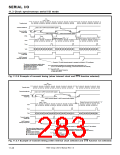
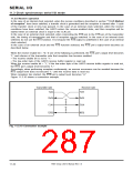
UART0 receive interrupt control register (Address 7216
UART1 receive interrupt control register (Address 7416
UART2 receive interrupt control register (Address F216
b7 b0
)
)
)
CLK polarity select bit
0: At the rising edge of the transfer
clock, receive data is input.
1: At the falling edge of the transfer
clock, receive data is input.
Interrupt priority level select bits
When using interrupts, set these bits to
one of levels 1 to 7.
When disabling interrupts, set these bits
to level 0.
Transfer format select bit
0: LSB first
1: MSB first
UART0 transmit buffer register (Address 3216
)
Serial I/O pin control register (Address AC16
)
UART1 transmit buffer register (Address 3A16
UART2 transmit buffer register (Address B216
)
)
b7 b0
b7
b0
CTS
0: CTS
CTS /RTS
0: CTS /RTS
TxD /P1 switch bit (Note 2)
0: Functions as TxD
1: Functions as P1
TxD /P1 switch bit (Note 2)
0: Functions as TxD
1: Functions as P1
CTS /RTS separate select bit
0: CTS /RTS are used together (Note 1)
TxD /P8 witch bit (Note 2)
0: Functions as TxD
1: Functions as P8
0
/RTS
/RTS
separate select bit
are used together (Note 1)
0
separate select bit
0
0
are used together (Note 1)
1
1
Dummy data is set.
1
1
1
0
3
0.
3.
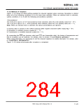
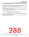
UART0 transmit/receive control register 1 (Address 3516
UART1 transmit/receive control register 1 (Address 3D16
UART2 transmit/receive control register 1 (Address B516
)
)
)
1
7
1.
7
7.
2
2
b7
b0
2
2
1
1
2
3 s3
2.
Transmit enable bit
3.
1: Transmission enabled
Reception enable bit
1: Reception enabled
Notes 1: In the clock synchronous serial I/O
mode, CTS /RTS separation cannot
i
i
be selected. (Refer to section “[Pre-
cautions for clock synchronous
serial I/O mode].”)
Note: Set the receive enable bit
and the transmit enable
bit to “1” simultaneously.
2: When only reception is performed, if
i
these bits = “1,” the TxDi pin can be
used as a programmable I/O port
pin.
Reception starts.
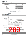
Fig. 11.3.8 Initial setting example for relevant registers when receiving
7905 Group User’s Manual Rev.1.0
11-30

 RENESAS [ RENESAS TECHNOLOGY CORP ]