PULSE OUTPUT PORT MODE
9.1 Overview
9.1 Overview
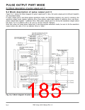
The pulse output port mode function is used to change the output levels at several pins simultaneously with
the following: each underflow occurrence in timer A or each valid edge input of an external signal. The pulse
output port mode consists of pulse output port 0 and pulse output port 1. These two circuits have the
equivalent functions and operate independently each other. Each of pulse output port 0 and pulse output
port 1 has two operation modes as listed in Table 9.1.1. Table 9.1.2 lists the overview of pulse output port
0; Table 9.1.3 lists the overview of pulse output port 1.
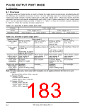
Table 9.1.1 Overview of pulse output port mode
Pulse output mode
Function
Pulse output port 0
Pulse mode 0
Pulse output port 1
Pulse mode 1
Pulse mode 0
Circuit
Operation mode
Pulse mode 1
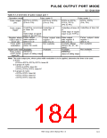
Table 9.1.2 Overview of pulse output port 0
Operation mode
Pulse mode 0
RTP1 to RTP1
(P6 to P6
Pulse mode 1
RTP1 , RTP1
(P6 , P6
RTP0
0
to RTP0
3
2
3
RTP0
RTP1
0
0
to RTP0
, RTP1
3
,
Pulse output
pins
0
3
(P6 to P6 )
0
3
4
7
)
4
7
)
1
(P6
0
to P6 )
5
Underflow occurrence
in timer A0
or
Valid edge of signal
input to pin RTPTRG0
Three-phase output
data register 0
(bits 0 to 3)
Underflow of timer A3
Underflow of timer A3 Underflow of timer A0
Pulse output
trigger
or
Valid edge of signal
input to pin RTPTRG0
Three-phase output
data register 1
(bits 6, 7)
Three-phase output Three-phase output
Register where
output data is
to be set
data register 1
(bits 4 to 7)
data register 0
(bits 0 to 5)
Available
(timer A1 used)
Not available
Not available
Available (Note)
(timers A1, A2, A4
used)
Pulse width
modulation
Available
P6OUTCUT
(Input of falling edge)
Not available
—
Negative pulse output
Pulse-output-
cutoff signal
input pin
Available
—
Available
P6OUTCUT
(Input of falling edge)
Note: The pulse output pins, where pulse width modulation is to be applied, determine the timer to be used.
➀➀6 pins
RTP0
0
to RTP0
3
, RTP1
0
, RTP1 : timer A1
1
➀ 2 groups of 3 pins
• RTP0
0
to RTP0
2
: timer A1
: timer A2
• RTP0
3
, RTP1 , RTP1
0
1
➀➀3 groups of 2 pins
• RTP0
• RTP0
• RTP1
0
2
0
, RTP0
1
: timer A1
: timer A2
: timer A4
, RTP0
3
, RTP1
1
7905 Group User’s Manual Rev.1.0
9-2

 RENESAS [ RENESAS TECHNOLOGY CORP ]