TIMER A
7.5 One-shot pulse mode
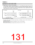
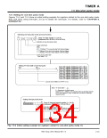
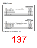
Timer A0 register (Addresses 4716, 4616)
Timer A1 register (Addresses 4916, 4816)
Timer A2 register (Addresses 4B16, 4A16)
Timer A3 register (Addresses 4D16, 4C16)
Timer A4 register (Addresses 4F16, 4E16)
Timer A5 register (Addresses C716, C616)
Timer A6 register (Addresses C916, C816)
Timer A7 register (Addresses CB16, CA16)
Timer A8 register (Addresses CD16, CC16)
Timer A9 register (Addresses CF16, CE16)
(b8)
b0 b7
(b15)
b7
b0
Bit
Function
Any value in the range from “000016” to “FFFF16” can be set.
At reset R/W
15 to 0
Undefined WO
Assuming that the set value = n, the “H” level width of the one-shot pulse which is
output from the TAiOUT pin is expressed as follows :
n
fi.
fi: Frequency of count source
Note: Use the MOVM or STA(STAD) instruction for writing to this register.
Writing to this register must be performed in a unit of 16 bits.
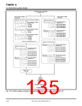
Timer Ai mode register (i = 0 to 4) (Addresses 5616 to 5A16)
Timer Ai mode register (i = 5 to 9) (Addresses D616 to DA16)
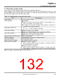
b7 b6 b5 b4 b3 b2 b1 b0
0
1 1 0
Function
1 0 : One-shot pulse mode
Bit
0
Bit name
At reset R/W
b1 b0
Operating mode select bits
0
0
0
0
RW
RW
RW
RW
1
2
3
Fix this bit to “1” in one-shot pulse mode.
b4 b3
Trigger select bits
0 0 :
0 1 :
Writing “1” to one-shot start bit
(TAiIN pin functions as a programmable I/O
port pin.)
4
0
RW
1 0 : Falling edge of TAiN pin’s input signal
1 1 : Rising edge of TAiIN pin’s input signal
5
6
Fix this bit to “0” in one-shot pulse mode.
See Table 7.2.3.
0
0
RW
RW
Count source select bits
7
0
RW
Fig. 7.5.1 Structures of timer Ai register and timer Ai mode register in one-shot pulse mode
7905 Group User’s Manual Rev.1.0
7-30

 RENESAS [ RENESAS TECHNOLOGY CORP ]