TIMER A
7.2 Block description
7.2 Block description
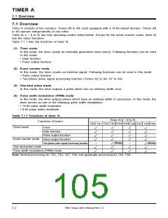
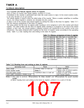
Figure 7.2.1 shows the block diagram of timer Ai (i = 0 to 9). Explanation of registers relevant to timer A
is described below.
Timer A clock division
select bits (Note)
Count source
select bit
f
2
f
1
Data bus (odd)
Data bus (even)
f
f
16
64
f
512
(Low-order 8 bits)
(High-order 8 bits)
f
4096
Timer mode
One-shot pulse mode
PWM mode
Timer Ai reload register (16)
Timer Ai counter (16)
Timer Ai
interrupt
request bit
Timer mode
(Gate function)
Event counter mode
Trigger
Polarity
switching
TAiN
Count start bit
Countup/Countdown
switching
(Always “countdown” except
for in the event counter
mode)
Countdown
Up-down bit
Pulse output
function select bit
Toggle
F.F.
TAiOUT
Note: Common to timers A0 to A9.
Fig. 7.2.1 Block diagram of timer Ai (i = 0 to 9)
7905 Group User’s Manual Rev.1.0
7-3

 RENESAS [ RENESAS TECHNOLOGY CORP ]