RTL8201CL
Datasheet
Name
RXER/
FXEN
Type
O/LI
Pin No.
Description
Receive Error.
24
If a 5B decode error occurs, such as invalid /J/K/, invalid /T/R/, or invalid
symbol, this pin will go high.
Fiber/UTP Enable.
During power on reset, this pin status is latched to determine the media mode to
operate in.
1: Fiber mode
0: UTP mode
An internal weak pull low resistor sets this to the default of UTP mode. It is possible
to use an external 5.1KΩ pull high resistor to enable fiber mode.
After power on, the pin operates as the Receive Error pin.
Management Data Clock.
This pin provides a clock synchronous to MDIO, which may be asynchronous
to the transmit TXC and receive RXC clocks. The clock rate can be up to
2.5MHz. An internal weak pull high resistor prevents the bus floating.
Management Data Input/Output.
MDC
I
25
26
MDIO
IO
This pin provides the bi-directional signal used to transfer management
information.
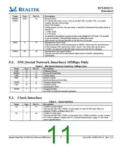
5.2. SNI (Serial Network Interface) 10Mbps Only
Table 2. SNI (Serial Network Interface) 10Mbps Only
Name
COL
Type
O
Pin No.
Description
Collision Detect.
1
RXD0
CRS
RXC
O
O
O
21
23
16
Received Serial Data.
Carrier Sense.
Receive Clock.
Resolved from received data.
Transmit Serial Data.
Transmit Clock.
TXD0
TXC
I
O
6
7
Generated by PHY.
TXEN
I
2
Transmit Enable.
For MAC to indicate transmit operation.
5.3. Clock Interface
Table 3. Clock Interface
Name
Type
Pin No.
Description
X2
O
47
25MHz Crystal Output.
This pin provides the 25MHz crystal output. It must be left open when an
external 25MHz oscillator drives X1.
X1
I
46
25MHz Crystal Input.
This pin provides the 25MHz crystal input. If a 25MHz oscillator is used, connect
X1 to the oscillator’s output (see 8.3 Crystal Characteristics, page 30, for clock
source specifications.
Single-Chip/Port 10/100 Fast Ethernet PHYceiver
5
Track ID: JATR-1076-21 Rev. 1.24

 REALTEK [ Realtek Semiconductor Corp. ]