FM25W256 - 256Kb SPI F-RAM
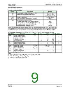
AC Parameters (TA = -40°C to + 85°C, VDD = 2.7V to 5.5V, CL = 30pF)
Symbol
fCK
tCH
tCL
Parameter
Min
0
Max
Units
MHz
ns
Notes
SCK Clock Frequency
Clock High Time
Clock Low Time
Chip Select Setup
Chip Select Hold
Output Disable Time
Output Data Valid Time
Output Hold Time
Deselect Time
Data In Rise Time
Data In Fall Time
Data Setup Time
Data Hold Time
20
22
22
10
10
1
1
ns
tCSU
tCSH
tOD
tODV
tOH
tD
ns
ns
20
20
ns
2
ns
0
60
ns
ns
tR
50
50
ns
2,3
2,3
tF
ns
tSU
5
5
10
10
ns
tH
ns
tHS
/Hold Setup Time
/Hold Hold Time
/Hold Low to Hi-Z
/Hold High to Data Active
ns
tHH
tHZ
tLZ
ns
25
20
ns
2
2
ns
Notes
1. tCH + tCL = 1/fCK
.
2. This parameter is characterized but not 100% tested.
3. Rise and fall times measured between 10% and 90% of waveform.
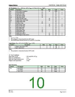
Capacitance (TA = 25° C, f=1.0 MHz, VDD = 5.0V)
Symbol
CO
Parameter
Min
-
-
Max
8
6
Units
pF
pF
Notes
1
1
Output Capacitance (SO)
Input Capacitance
CI
Notes
1. This parameter is characterized and not 100% tested.
AC Test Conditions
Input Pulse Levels
10% and 90% of VDD
Input rise and fall times
Input and output timing levels
Output Load Capacitance
5 ns
0.5 VDD
30 pF
Data Retention
Symbol
Parameter
Min
10
Max
Units
Years
Years
Years
Notes
TDR
@
@
@
+85ºC
+80ºC
+75ºC
-
-
-
19
38
Rev. 1.3
Feb. 2011
Page 10 of 13

 RAMTRON [ RAMTRON INTERNATIONAL CORPORATION ]