FM25W256 - 256Kb SPI F-RAM
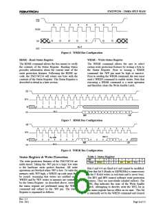
CS
0
1
2
3
4
5
1
6
0
7
SCK
0
0
0
0
0
0
SI
Hi-Z
SO
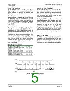
Figure 6. WRDI Bus Configuration
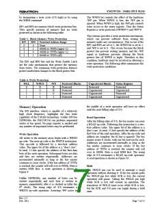
RDSR – Read Status Register
WRSR – Write Status Register
The RDSR command allows the bus master to verify
the contents of the Status Register. Reading Status
provides information about the current state of the
write protection features. Following the RDSR op-
code, the FM25W256 will return one byte with the
contents of the Status Register. The Status Register is
described in detail in a later section.
The WRSR command allows the user to select
certain write protection features by writing a byte to
the Status Register. Prior to issuing a WRSR
command, the /WP pin must be high or inactive.
Prior to sending the WRSR command, the user must
send a WREN command to enable writes. Note that
executing a WRSR command is a write operation
and therefore clears the Write Enable Latch.
Figure 7. RDSR Bus Configuration
Figure 8. WRSR Bus Configuration
Table 2. Status Register
Status Register & Write Protection
7
6
0
5
0
4
0
3
BP1
2
BP0
1
0
0
Bit
The write protection features of the FM25W256 are
multi-tiered. Taking the /WP pin to a logic low state
is the hardware write protect function. All write
operations are blocked when /WP is low. To write the
memory with /WP high, a WREN op-code must first
be issued. Assuming that writes are enabled using
WREN and by /WP, writes to memory are controlled
by the Status Register. As described above, writes to
the status register are performed using the WRSR
command and subject to the /WP pin. The Status
Register is organized as follows.
WPEN
WEL
Name
Bits 0 and 4-6 are fixed at 0 and cannot be modified.
Note that bit 0 (Ready in EEPROMs) is unnecessary
as the F-RAM writes in real-time and is never busy.
The BP1 and BP0 control software write protection
features. They are nonvolatile (shaded yellow). The
WEL flag indicates the state of the Write Enable
Latch. Attempting to directly write the WEL bit in
the status register has no effect on its state. This bit
is internally set by the WREN command and cleared
Rev. 1.3
Feb. 2011
Page 6 of 13

 RAMTRON [ RAMTRON INTERNATIONAL CORPORATION ]