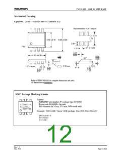
FM25L16B - 16Kb 3V SPI F-RAM
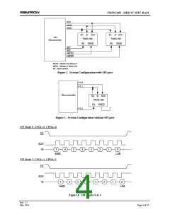
CS
0
1
2
3
4
5
6
7
0
1
2
3
4
5
6
4
3
5
6
7
0
1
2
3
4
5
6
7
SCK
op-code
11-bit Address
10
Data
X
X
X
X
X
9
2
1
0
7
6
5
4
3
2
1
0
SI
0
0
0
0
0
0
1
0
MSB
LSB MSB
LSB
SO
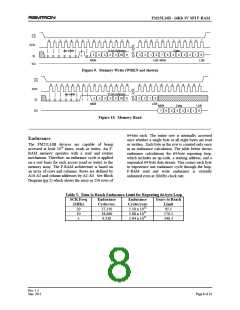
Figure 9. Memory Write (WREN not shown)
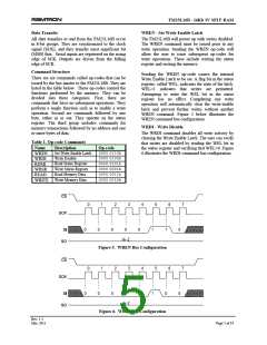
CS
0
1
2
3
4
5
6
7
0
1
2
3
4
5
6
4
5
6
7
0
1
2
3
4
5
6
7
SCK
SI
op-code
11-bit Address
10
X
X
X
X
X
9
3
2
1
0
0
0
0
0
0
0
1
1
MSB
LSB
Data
MSB
7
LSB
SO
6
5
4
3
2
1
0
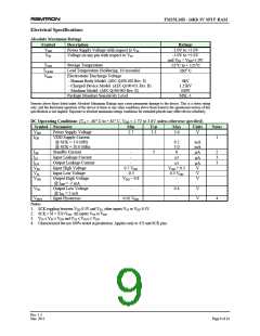
Figure 10. Memory Read
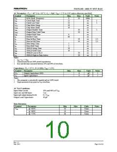
64-bits each. The entire row is internally accessed
once whether a single byte or all eight bytes are read
or written. Each byte in the row is counted only once
in an endurance calculation. The table below shows
endurance calculations for 64-byte repeating loop,
which includes an op-code, a starting address, and a
sequential 64-byte data stream. This causes each byte
to experience one endurance cycle through the loop.
F-RAM read and write endurance is virtually
unlimited even at 20MHz clock rate.
Endurance
The FM25L16B devices are capable of being
accessed at least 1014 times, reads or writes. An F-
RAM memory operates with a read and restore
mechanism. Therefore, an endurance cycle is applied
on a row basis for each access (read or write) to the
memory array. The F-RAM architecture is based on
an array of rows and columns. Rows are defined by
A10-A3 and column addresses by A2-A0. See Block
Diagram (pg 2) which shows the array as 256 rows of
Table 5. Time to Reach Endurance Limit for Repeating 64-byte Loop
SCK Freq Endurance Endurance Years to Reach
(MHz) Cycles/sec. Limit
Cycles/year
20
10
5
37,310
18,660
9,330
1.18 x 10¹²
5.88 x 10¹¹
2.94 x 10¹¹
85.1
170.2
340.3
Rev. 1.3
Mar. 2011
Page 8 of 14

 RAMTRON [ RAMTRON INTERNATIONAL CORPORATION ]