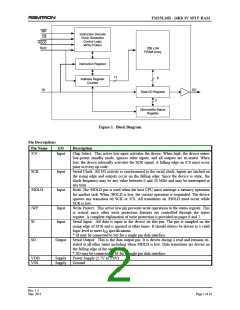
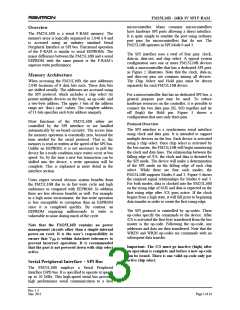
FM25L16B - 16Kb 3V SPI F-RAM
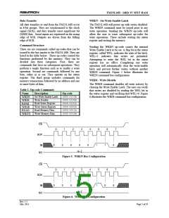
WRSR – Write Status Register
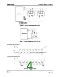
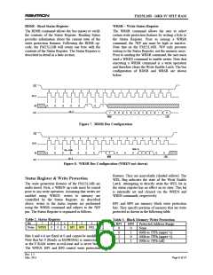
RDSR - Read Status Register
The RDSR command allows the bus master to verify
the contents of the Status Register. Reading Status
provides information about the current state of the
write protection features. Following the RDSR op-
code, the FM25L16B will return one byte with the
contents of the Status Register. The Status Register is
described in detail in a later section.
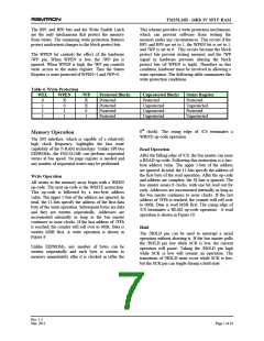
The WRSR command allows the user to select
certain write protection features by writing a byte to
the Status Register. Prior to issuing a WRSR
command, the /WP pin must be high or inactive.
Note that on the FM25L16B, /WP only prevents
writing to the Status Register, not the memory array.
Prior to sending the WRSR command, the user must
send a WREN command to enable writes. Note that
executing a WRSR command is a write operation
and therefore clears the Write Enable Latch. The bus
configuration of RDSR and WRSR are shown
below.
Figure 7. RDSR Bus Configuration
Figure 8. WRSR Bus Configuration (WREN not shown)
features. They are nonvolatile (shaded yellow). The
Status Register & Write Protection
WEL flag indicates the state of the Write Enable
Latch. Attempting to directly write the WEL bit in
the status register has no effect on its state. This bit
is internally set and cleared via the WREN and
WRDI commands, respectively.
The write protection features of the FM25L16B are
multi-tiered. First, a WREN op-code must be issued
prior to any write operation. Assuming that writes are
enabled using WREN, writes to memory are
controlled by the Status Register. As described
above, writes to the status register are performed
using the WRSR command and subject to the /WP
pin. The Status Register is organized as follows.
BP1 and BP0 are memory block write protection
bits. They specify portions of memory that are write
protected as shown in the following table.
Table 2. Status Register
Table 3. Block Memory Write Protection
Bit
7
6
5
4
0
3
2
1
0
0
BP1
BP0 Protected Address Range
Name WPEN
0
0
BP1
BP0
WEL
0
0
1
1
0
1
0
1
None
600h to 7FFh (upper ¼)
400h to 7FFh (upper ½)
000h to 7FFh (all)
Bits 0 and 4-6 are fixed at 0 and cannot be modified.
Note that bit 0 (Ready in EEPROMs) is unnecessary
as the F-RAM writes in real-time and is never busy.
The WPEN, BP1 and BP0 control write protection
Rev. 1.3
Mar. 2011
Page 6 of 14

 RAMTRON [ RAMTRON INTERNATIONAL CORPORATION ]