FM24CL16B - 16Kb 3V I2C F-RAM
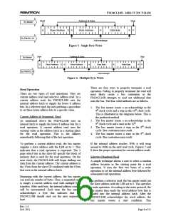
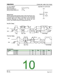
Start
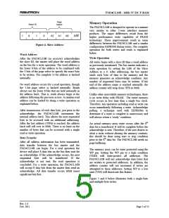
S
Address & Data
Word Address
Stop
By Master
Slave Address
0
A
A
Data Byte
A
P
By FM24CL16
Acknowledge
Figure 5. Single Byte Write
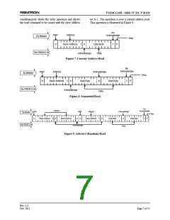
Start
Address & Data
Stop
P
By Master
S
Slave Address
0
A
Word Address
A
Data Byte
A
Data Byte
A
By FM24CL16
Acknowledge
Figure 6. Multiple Byte Write
There are four ways to properly terminate a read
operation. Failing to properly terminate the read will
Read Operation
There are two types of read operations. They are
current address read and selective address read. In a
current address read, the FM24CL16B uses the
internal address latch to supply the lower 8 address
bits. In a selective read, the user performs a procedure
to set these lower address bits to a specific value.
most likely create
a
bus contention as the
FM24CL16B attempts to read out additional data
onto the bus. The four valid methods are as follows.
1. The bus master issues a no-acknowledge in the
9th clock cycle and a stop in the 10th clock cycle.
This is illustrated in the diagrams below. This is
the preferred method.
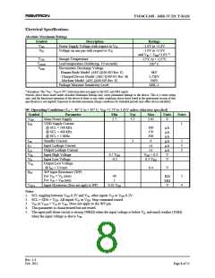
Current Address & Sequential Read
2. The bus master issues a no-acknowledge in the
As mentioned above the FM24CL16B uses an
internal latch to supply the lower 8 address bits for a
read operation. A current address read uses the
existing value in the address latch as a starting place
for the read operation. This is the address
immediately following that of the last operation.
9th clock cycle and a start in the 10th.
3. The bus master issues a stop in the 9th clock
cycle. Bus contention may result.
4. The bus master issues a start in the 9th clock
cycle. Bus contention may result.
If the internal address reaches 7FFh it will wrap
around to 000h on the next read cycle. Figures 7 and
8 show the proper operation for current address reads.
To perform a current address read, the bus master
supplies a slave address with the LSB set to 1. This
indicates that a read operation is requested. The 3
page select bits in the slave ID specify the block of
memory that is used for the read operation. On the
next clock, the FM24CL16B will begin shifting out
data from the current address. The current address is
the 3 bits from the slave ID combined with the 8 bits
that were in the internal address latch.
Selective (Random) Read
A simple technique allows a user to select a random
address location as the starting point for a read
operation. It uses the first two bytes of a write
operation to set the internal address byte followed by
subsequent read operations.
Beginning with the current address, the bus master
can read any number of bytes. Thus, a sequential read
is simply a current address read with multiple byte
transfers. After each byte, the internal address counter
will be incremented. Each time the bus master
To perform a selective read, the bus master sends out
the slave address with the LSB set to 0. This specifies
a write operation. According to the write protocol, the
bus master then sends the word address byte that is
loaded into the internal address latch. After the
FM24CL16B acknowledges the word address, the
acknowledges
a
byte this indicates that the
FM24CL16B should read out the next sequential
byte.
bus master issues
a
start condition. This
Rev. 1.4
Feb. 2011
Page 6 of 13

 RAMTRON [ RAMTRON INTERNATIONAL CORPORATION ]