FM24CL16B - 16Kb 3V I2C F-RAM
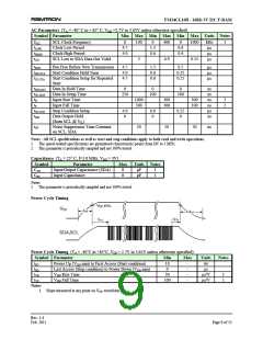
AC Test Conditions
Equivalent AC Load Circuit
Input Pulse Levels
0.1 VDD to 0.9 VDD
10 ns
3.6V
Input rise and fall times
Input and output timing levels
0.5 VDD
1100 Ω
Output
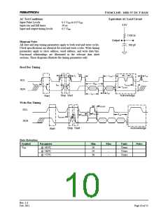
Diagram Notes
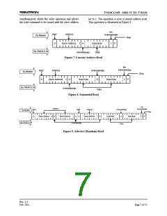
All start and stop timing parameters apply to both read and write cycles.
Clock specifications are identical for read and write cycles. Write timing
parameters apply to slave address, word address, and write data bits.
Functional relationships are illustrated in the relevant data sheet
sections. These diagrams illustrate the timing parameters only.
100 pF
Read Bus Timing
tHIGH
tR
tSP
tF
t SP
tLOW
`
SCL
SDA
1/fSCL
tSU:STA
tHD:DAT
tSU:DAT
tBUF
tDH
tAA
Stop Start
Acknowledge
Start
Write Bus Timing
tHD:DAT
SCL
tSU:DAT
tAA
tHD:STA
tSU:STO
SDA
Stop Start
Acknowledge
Start
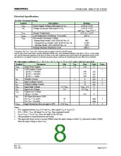
Data Retention
Symbol
Parameter
Min
Max
Units
Years
Years
Years
Notes
TDR
@
@
@
+85ºC
+80ºC
+75ºC
10
19
38
-
-
-
Rev. 1.4
Feb. 2011
Page 10 of 13

 RAMTRON [ RAMTRON INTERNATIONAL CORPORATION ]