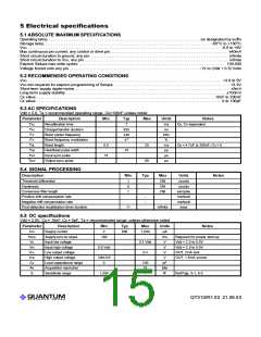
During fast integration (Section 2.5), when bursts are
generated quickly a number of times in sequence without
regard to the sleep timer, a single SYNC_O pulse is
It is also possible to devise a tree structure of devices, where
some devices in the chain trigger two or more slaves. This
speeds up the acquisition process considerably, but some
generated only after the last burst in the series of fast spaced thought must be given to timing considerations so that
adjacent electrodes do not have bursts which overlap each
other in time.
bursts in order to prevent downstream slave parts from being
triggered too rapidly.
If SC=0 (no sleep cycles), no Sync_O pulses are generated.
After the burst has completed the QT310 checks the level on
SYNC_I. If SYNC_I is high, the part goes back to sleep; if
SYNC_I is still low the device waits until the SYNC_I is high
again before going back to sleep. If this is the case, power
drain will be higher so it is important to limit the pulse width to
an amount less than the burst length (but greater than
>15µs).
Disabling Sync: Connecting Sync_I to +Vdd will disable Sync
and the part will acquire bursts at the normal rate. If Sync is at
Vss, the device will wait for a Sync pulse, until the Tsc period
Vdd
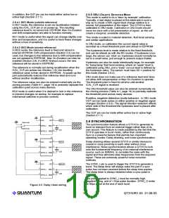
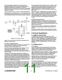
2.9.2 NOISE
S
YNCHRONIZATION
U2:A
74HC14
C1
100pF
Using the sync feature, a QT310 can be synchronized to a
repetitive external source of interference such as the power
line frequency (Figure 2-4) in order to dramatically reduce
signal noise. If line frequency is present near the sensors, this
feature should be used.
R1
1M
R3
1M
R4
4.7k - 10K
R2
470K-1M
Line Input
2.2nF
C2
Vdd
U1
With this circuit the sensor can tolerate up to 100V/M of AC
electric field. It is particularly useful for line-powered touch
controls.
8
VDD
7
1
6
2
OUT1
OUT
/CAL
Noise sync and daisy-chaining can be combined by having
the first device in the chain sync to the external noise source.
3
5
SENSOR
SNS1
SNS2
/SYNC_I
CS
/SYNC_O
/SYNC_O
3 Circuit Guidelines
VSS
3.1 SAMPLE CAPACITORS
4
Cs capacitors can be virtually any plastic film or low to
medium-K ceramic capacitor. The normal usable Cs range is
from 10nF ~ 200nF depending on the sensitivity required;
larger values of Cs require higher stability to ensure reliable
sensing. Acceptable capacitor types include NP0 or C0G
ceramic, PPS film, Polypropylene film, and X7R ceramic in
that order.
Figure 2-4 Line sync circuit
expires; at that point the part will acquire regardless of the
absence of a Sync pulse.
2.9.1 DAISY-CHAINING QT310’
S
3.2 POWER SUPPLY
One use for synchronization is where two or more QT310’s in
close proximity to each other are synchronously daisy-
chained to avoid crosstalk (Figure 2-3).
3.2.1 STABILITY
The QT310 derives its internal references from the power
supply. Sensitivity shifts and timing changes will occur with
changes in Vdd, as often happens when additional power
supply loads are switched on or off via the Out pin.
One QT310 should be designated as the ‘Master’; this part
should have the shortest SC sleep time, while the
downstream parts which depend on the master and any
intermediary devices should have longer sleep time settings
than the master.
These supply shifts can induce detection ‘cycling’, whereby an
object is detected, the load is turned on, the supply sags, the
detection is no longer sensed, the load is turned off, the
supply rises and the object is reacquired, ad infinitum.
The parts can be chained in a loop (Fig 2-4 switch set to
‘closed loop’); in this configuration the master will generate a
new burst after the last slave has finished, making the scan
sequence of all devices the most time-efficient possible. If the
master doesn’t received a pulse before the sleep time has
elapsed it will generate a new burst. This mode is most useful
if there are a relatively small number of devices in the chain
and there is a need for fast response.
Detection ‘stiction’, the opposite effect, can occur if a load is
shed when the output is active and the signal swings are
small: the Out pin can remain stuck even if the detected
object is no longer near the electrode.
3.2.2 SUPPLY
R
EQUIREMENTS
In open-loop, the rep rate of acquisition is set purely by the
burst rate of the master. It is possible in this mode to have
very long chains of parts with relatively good response time.
The disadvantage of this mode is that it is possible for the
bursts of downstream slaves to overlap with upstream
devices, potentially causing interference if their electrodes are
in physical proximity to each other.
Vdd can range from 2.0 to 5.0 volts. If Setups programming is
required during operation, the minimum Vdd is 2.2V. Current
drain will vary depending on Vdd, the chosen sleep cycles,
and the burst lengths. Increasing Cx values will decrease
power drain since increasing Cx loads decrease burst length
(Figures 5-1 and 5-2).
LQ
11
QT310/R1.03 21.09.03

 QUANTUM [ QUANTUM RESEARCH GROUP ]