If the power supply is shared with another electronic system,
care should be taken to assure that the supply is free of
spikes, sags, and surges. In BG1 mode the QT310 will track
slow changes in Vdd if drift compensation is enabled, but it
can be adversely affected by rapid voltage steps and spikes
at the millivolt level.
VDD
100nF
8
VDD
RE3
RE4
RE5
RE2
RE1
1
2
6
7
3
5
CAL
OUT
If desired, the supply can be regulated using a conventional
low current regulator, for example CMOS LDO regulators with
low quiescent currents, or standard 78Lxx-series 3-terminal
regulators.
SYNC_O SNS1
SYNC_I SNS2
SENSOR
CS
For proper operation a 100nF (0.1uF) ceramic bypass
capacitor must be used between Vdd and Vss; the bypass
cap should be placed very close to the Vdd and Vss pins.
VSS
4
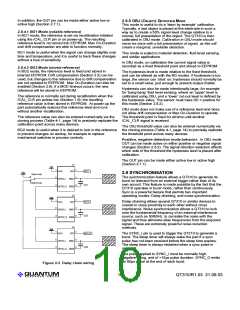
Figure 3-1 ESD/EMC protection resistors
3.3 PCB LAYOUT
3.3.1 GROUND
P
LANES
dielectric properties, panel thickness, and rise time of the
ESD transients.
The use of ground planes around the device is encouraged
for noise reasons, but ground should not be coupled too close
to the sense pins in order to reduce Cx load. Likewise, the
traces leading from the sense pins to the electrode should not
be placed directly over a ground plane; rather, the ground
plane should be relieved by at least 3 times the width of the
sense traces directly under it, with periodic thin bridges over
the gap to provide ground continuity.
ESD protection can be enhanced with an added resistor RE1
(Figure 3-1). As the transfer time is ~833ns, the circuit can
tolerate values of RE1 which result in an RC timeconstant of
1/6th this amount or about 140ns. The ‘C’ of the RC is the Cx
load. Thus, for Cx= 20pF, the maximum of RE1 should be
6.8K ohms. Larger amounts of RE1 or Cx may result in
noticeably reduced gain.
3.3.2 CLONE
P
ORT
C
ONNECTOR
If a cloning connector is used, place this close to the QT310.
Placing the cloning connector far from the QT310 will increase
the load capacitance Cx of the sensor line SNS1 and
decrease sensitivity. Long distances on these lines can also
make the cloning process more susceptible to communication
errors from ringing and interference.
3.5 EMC ISSUES
Electromagnetic and electrostatic susceptibility are often a
problem with capacitive sensors. QT310 behavior under these
conditions can be improved by adding RE1 (Figure 3-1),
exactly as for ESD protection. The resistor should be placed
next to the chip.
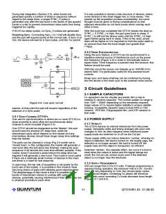
If the SYNC_I input is used, a 10K ohm resistor should be
used to avoid conflicts with the cloning process (Figure 4-1).
This works because the inbound RC network formed by RE1
and Cs has a very low cut-off frequency which can be
computed by the formula:
Cloning can be designed for production by using pads (SMT
or through-hole) on the solder side which are connected to a
fixture via spring loaded ATE-style ‘pogo-pins’. This eliminates
the need for an actual connector to save cost.
1
Fc =
2✜ RCs
If R = 6.8K and Cs = 10nF, then Fc = 2,340 Hz.
Important Note: Since SCK is shared on the SNS1 pin, it is
possible that stray external fields can cause these devices to
enter into Clone mode accidentally. If long wiring or large
electrodes are used that could pick up interference, install a
470K resistor from SNS1 to ground to suppress pickup. If the
device enters clone mode accidentally, it may be necessary to
cycle power to recover the device.
This leads to very strong suppression of external field effects.
Nevertheless, it is always wise to reduce lead lengths by
placing the QT310 as close to the electrode as possible.
3.4 ESD ISSUES
VDD
In cases where the electrode is placed behind a dielectric
panel, the device will usually be well protected from static
discharge. However, even with a plastic or glass panel,
transients can still flow into the electrode via induction, or in
extreme cases, via dielectric breakdown. Porous materials
may allow a spark to tunnel right through the material; partially
conducting materials like 'pink poly' static dissipative plastics
will conduct the ESD right to the electrode. Panel seams can
permit discharges through edges or cracks.
100nF
8
VDD
1
2
6
7
3
5
/CAL
/SYNC_O
/SYNC_I
C/AL
SDI
SCK
OUT
SENSOR
S/YNC_O
SDO
CS
SNS2
Testing is required to reveal any problems. The QT310 has
internal diode protection which can absorb and protect the
device from most induced discharges, up to 20mA; the
usefulness of the internal clamping will depend on the
VSS
4
Figure 4-1 Clone interface wiring
LQ
12
QT310/R1.03 21.09.03

 QUANTUM [ QUANTUM RESEARCH GROUP ]