PE43704
Product Specification
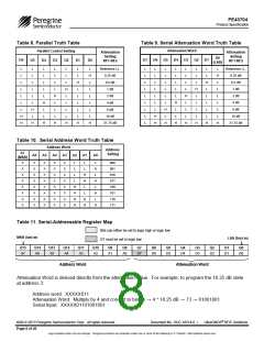
Programming Options
Parallel/Serial Selection
The shift register must be loaded while LE is held
LOW to prevent the attenuator value from changing
as data is entered. The LE input should then be
toggled HIGH and brought LOW again, latching the
new data into the DSA. Attenuation Word and
Address Word truth tables are listed in Table 9 and
Table 10. A programming example of the serial
register is illustrated in Table 11. The serial timing
diagram is illustrated in Figure 5.
Either a parallel or serial-addressable interface can be
used to control the PE43704. The P/S bit provides this
selection, with P/S = LOW selecting the parallel
interface and P/S = HIGH selecting the serial-
addressable interface.
Parallel Mode Interface
Power-up Control Settings
The parallel interface consists of seven CMOS-
compatible control lines that select the desired
attenuation state, as shown in Table 8.
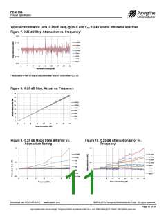
The PE43704 will always initialize to the maximum
attenuation setting (31.75 dB) on power-up for both
the serial-addressable and latched-parallel modes
of operation and will remain in this setting until the
user latches in the next programming word. In direct
-parallel mode, the DSA can be preset to any state
within the 31.75 dB range by pre-setting the parallel
control pins prior to power-up. In this mode, there is
a 400-µs delay between the time the DSA is
powered-up to the time the desired state is set.
During this power-up delay, the device attenuates
to the maximum attenuation setting (31.75 dB)
before defaulting to the user defined state. If the
control pins are left floating in this mode during
power-up, the device will default to the minimum
attenuation setting (insertion loss state).
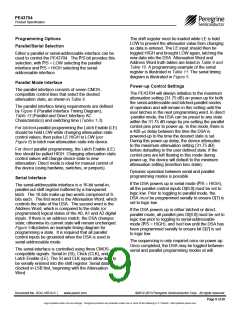
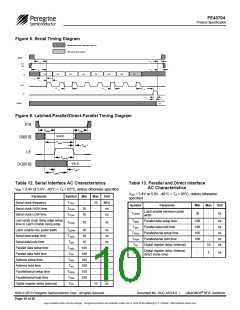
The parallel interface timing requirements are defined
by Figure 6 (Parallel Interface Timing Diagram),
Table 13 (Parallel and Direct Interface AC
Characteristics) and switching time (Tables 1-3).
For latched-parallel programming the Latch Enable (LE)
should be held LOW while changing attenuation state
control values, then pulse LE HIGH to LOW (per
Figure 6) to latch new attenuation state into device.
For direct parallel programming, the Latch Enable (LE)
line should be pulled HIGH. Changing attenuation state
control values will change device state to new
attenuation. Direct mode is ideal for manual control of
the device (using hardwire, switches, or jumpers).
Dynamic operation between serial and parallel
programming modes is possible.
Serial Interface
If the DSA powers up in serial mode (P/S = HIGH),
all the parallel control inputs DI[6:0] must be set to
logic low. Prior to toggling to parallel mode, the
DSA must be programmed serially to ensure D[7] is
set to logic low.
The serial-addressable interface is a 16-bit serial-in,
parallel-out shift register buffered by a transparent
latch. The 16-bits make up two words comprised of 8-
bits each. The first word is the Attenuation Word, which
controls the state of the DSA. The second word is the
Address Word, which is compared to the static (or
programmed) logical states of the A0, A1 and A2 digital
inputs. If there is an address match, the DSA changes
state; otherwise its current state will remain unchanged.
Figure 5 illustrates an example timing diagram for
programming a state. It is required that all parallel
control inputs be grounded when the DSA is used in
serial-addressable mode.
If the DSA powers up in either latched or direct-
parallel mode, all parallel pins DI[6:0] must be set to
logic low prior to toggling to serial-addressable
mode (P/S = HIGH), and held low until the DSA has
been programmed serially to ensure bit D[7] is set
to logic low.
The sequencing is only required once on power-up.
Once completed, the DSA may be toggled between
serial and parallel programming modes at will.
The serial-interface is controlled using three CMOS-
compatible signals: Serial-In (SI), Clock (CLK), and
Latch Enable (LE). The SI and CLK inputs allow data to
be serially entered into the shift register. Serial data is
clocked in LSB first, beginning with the Attenuation
Word.
Document No. DOC-16514-6 |
www.psemi.com
©2012-2013 Peregrine Semiconductor Corp. All rights reserved.
Page 9 of 20
Logo updated under non-rev change. Peregrine products are protected under one or more of the following U.S. Patents: http://patents.psemi.com

 PSEMI [ Peregrine Semiconductor ]