PE43704
Product Specification
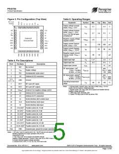
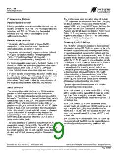
Figure 3. Pin Configuration (Top View)
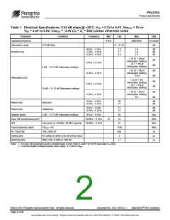
Table 5. Operating Ranges
Symbol
Parameter
Min
Typ
Max Unit
Supply voltage (normal
mode, VssEXT = 0V)1
VDD
2.3
5.5
V
Supply voltage (bypass
mode, VssEXT = -3.4V,
VDD≥3.4V for full spec.
compliance)2
VDD
2.7
3.4
5.5
V
Negative supply voltage
(bypass mode)2
VssEXT
IDD
-3.6
-2.4
200
80
V
Supply current (normal
mode, VssEXT = 0V)1
130
50
μA
μA
Supply current (bypass
mode, VssEXT = -3.4V)2
IDD
Negative supply current
(bypass mode, VssEXT
=
ISS
-40
-16
μA
-3.4V)2
Digital input high
Digital input low
VIH
VIL
1.17
-0.3
3.6
0.6
15
V
V
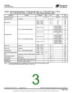
Table 4. Pin Descriptions
Pin #
Pin Name
N/C
Description
Digital input current
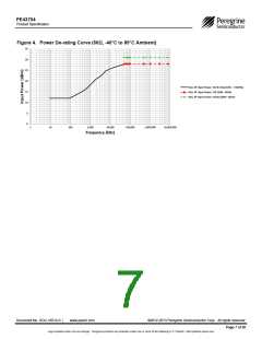
RF input power, CW3
ICTRL
μA
1
2
3
4
No connect
see
Fig. 4 dBm
+28 dBm
VDD
Supply voltage
9 kHz < 50 MHz
50 MHz ≤8 GHz
PMAX,CW
P/S
Serial/parallel mode select
Address bit A0 connection
RF input power, pulsed4
see
Fig. 4 dBm
+31 dBm
A0
9 kHz < 50 MHz PMAX,PULSED
50 MHz ≤8 GHz
5, 6,
8-17, 19
GND
Ground
Operating temperature
range
TOP
-40
25
+85
°C
7
18
20
21
22
23
24
25
26
27
28
29
30
31
32
Pad
RF11
RF21
RF1 port (RF input)
Notes: 1. Normal mode: connect VssEXT (pin 20) to GND (VssEXT = 0V) to
enable internal negative voltage generator
RF2 port (RF output)
2
2. Bypass mode: use VssEXT (pin 20) to bypass and disable internal
negative voltage generator
3. 100% duty cycle, all bands, 50Ω
VssEXT
External Vss negative voltage control
Address bit A2 connection
Address bit A1 connection
Serial interface latch enable input
Serial interface clock input
Serial interface data input
A2
A1
4. Pulsed, 5% duty cycle of 4620 µs period, 50Ω
LE
CLK
SI
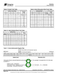
C16 (D6)3 Parallel control bit, 16 dB
C8 (D5)3
C4 (D4)3
C2 (D3)3
C1 (D2)3
Parallel control bit, 8 dB
Parallel control bit, 4 dB
Parallel control bit, 2 dB
Parallel control bit, 1 dB
C0.5 (D1)3 Parallel control bit, 0.5 dB
C0.25 (D0)3 Parallel control bit, 0.25 dB
GND
Exposed pad: ground for proper operation
Notes: 1. RF pins 7 and 18 must be at 0V DC. The RF pins do not require DC
blocking capacitors for proper operation if the 0V DC
requirement is met
2. Use VssEXT (pin 20) to bypass and disable internal
negative voltage generator. Connect VssEXT (pin 20) to GND (VssEXT = 0V)
to enable internal negative voltage generator
3. Ground C0.25, C0.5, C1 C2, C4, C8, C16 if not in use
Document No. DOC-16514-6 |
www.psemi.com
©2012-2013 Peregrine Semiconductor Corp. All rights reserved.
Page 5 of 20
Logo updated under non-rev change. Peregrine products are protected under one or more of the following U.S. Patents: http://patents.psemi.com

 PSEMI [ Peregrine Semiconductor ]