PE43704
Product Specification
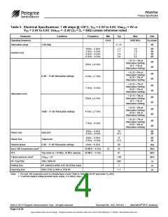
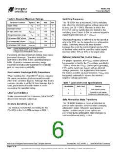
Table 6. Absolute Maximum Ratings
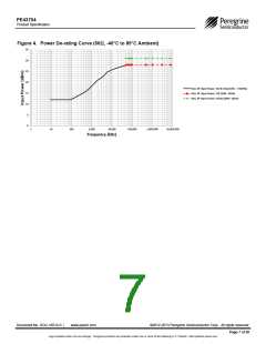
Switching Frequency
Parameter/Condition
Supply voltage
Symbol Min
Max
5.5
Unit
V
The PE43704 has a maximum 25 kHz switching
rate when the internal negative voltage generator
is used (pin 20 = GND). The rate at which the
PE43704 can be switched is only limited to the
switching time (Tables 1-3) if an external negative
supply is provided (pin 20 = VssEXT).
VDD
VCTRL
-0.3
-0.3
Digital input voltage
RF input power, max
3.6
V
PMAX,ABS
+34
dBm
Storage temperature range
ESD voltage HBM1, all pins
ESD voltage MM2, all pins
TST
-65
+150
1500
200
°C
V
VESD,HBM
VESD,MM
Switching frequency is defined to be the speed at
which the DSA can be toggled across attenuation
states. Switching time is the time duration
V
ESD voltage CDM3, all pins
VESD,CDM
250
V
between the point the control signal reaches 50%
of the final value and the point the output signal
reaches within 10% or 90% of its target value.
Notes: 1. Human Body Model (MIL-STD 883 Method 3015)
2. Machine Model (JEDEC JESD22-A115)
3. Charged Device Model (JEDEC JESD22-C101)
Exceeding absolute maximum ratings may cause
permanent damage. Operation should be
restricted to the limits in the Operating Ranges
table. Operation between operating range
maximum and absolute maximum for extended
periods may reduce reliability.
Optional External Vss Control (VssEXT
)
For proper operation, the VssEXT control pin must
be grounded or tied to the Vss voltage specified in
Table 5. When the VssEXT control pin is grounded,
FETs in the switch are biased with an internal
voltage generator. For applications that require
the lowest possible spur performance, VssEXT can
be applied externally to bypass the internal
negative voltage generator.
Electrostatic Discharge (ESD) Precautions
When handling this UltraCMOS® device, observe
the same precautions that you would use with
other ESD-sensitive devices. Although this device
contains circuitry to protect it from damage due to
ESD, precautions should be taken to avoid
exceeding the specified rating.
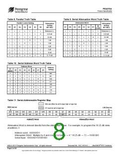
Table 7. Latch and Clock Specifications
Shift Clock
Latch Enable
Function
0
↑
Shift register clocked
Contents of shift register
transferred to attenuator core
Latch-Up Avoidance
↑
X
Unlike conventional CMOS devices, UltraCMOS®
devices are immune to latch-up.
Safe Attenuation State Transitions
The PE43704 features a novel architecture to
provide safe transition behavior when changing
attenuation states. When RF input power is
applied, positive output power spikes are
prevented during attenuation state changes by
optimized internal timing control.
Moisture Sensitivity Level
The Moisture Sensitivity Level rating for the
PE43704 in the 5x5 QFN package is MSL1.
©2012-2013 Peregrine Semiconductor Corp. All rights reserved.
Document No. DOC-16514-6 |
UltraCMOS® RFIC Solutions
Page 6 of 20
Logo updated under non-rev change. Peregrine products are protected under one or more of the following U.S. Patents: http://patents.psemi.com

 PSEMI [ Peregrine Semiconductor ]