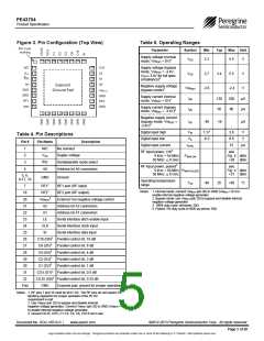
PE43704
Product Specification
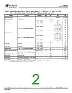
Table 1. Electrical Specifications: 0.25 dB steps @ +25°C, VDD = 2.3V to 5.5V, VssEXT = 0V or
VDD = 3.4V to 5.5V, VssEXT = -3.4V (ZS = ZL = 50Ω) unless otherwise noted
Parameter
Operating frequency
Attenuation range
Condition
Frequency
Min
Typ
Max
Unit
As shown
dB
9 kHz
6000 MHz
0.25 dB Step
0 – 31.75
9 kHz – 2 GHz
2 GHz – 4 GHz
4 GHz – 6 GHz
1.3
1.7
2.4
1.4
1.9
2.7
dB
dB
dB
Insertion loss
+ (0.15 + 3% of
Attenuation Setting)
- (0.1 + 1% of
dB
dB
9 KHz ≤4 GHz
4 GHz – 6 GHz
9 KHz ≤4 GHz
4 GHz – 6 GHz
Attenuation Setting)
0 dB – 15.75 dB Attenuation settings
+ (0.15 + 5% of
Attenuation Setting)
- 0.15
dB
dB
Attenuation error
+ (0.15 + 3%
Attenuation Setting)
- (0.1 + 1% of
dB
dB
Attenuation Setting)
16 dB – 31.75 dB Attenuation settings
+ (0.25 + 5% of
Attenuation Setting)
0.0
dB
dB
9 kHz – 4 GHz
4 GHz – 6 GHz
20
15
dB
dB
Return loss
Return loss
Input port
9 kHz – 4 GHz
4 GHz – 6 GHz
17
13
dB
dB
Output port
Relative phase
Input 1dB compression point1
IIP3
0 dB – 31.75 dB Attenuation settings
9 kHz – 6 GHz
50 MHz – 6 GHz
50 MHz – 6 GHz
58
34
deg
dBm
dBm
dBm
ns
32
Two tones at +18 dBm, 20 MHz spacing
VssEXT = 0V
61
Typical spurious value2
–140
600
2
RF Trise/Tfall
10% / 90% RF
Settling time
RF settled to within 0.05 dB of final value
50% CTRL to 90% or 10% RF
µs
Switching time
1.1
µs
Notes: 1. The input 1dB compression point is a linearity figure of merit. Refer to Table 5 for the RF input power PIN (50Ω)
2. To prevent negative voltage generator spurs, supply –3.4 volts to VssEXT
©2012-2013 Peregrine Semiconductor Corp. All rights reserved.
Document No. DOC-16514-6 |
UltraCMOS® RFIC Solutions
Page 2 of 20
Logo updated under non-rev change. Peregrine products are protected under one or more of the following U.S. Patents: http://patents.psemi.com

 PSEMI [ Peregrine Semiconductor ]