TOP242-249
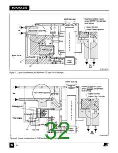
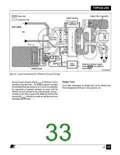
Output Filter Capacitors
Solder Side
Safety Spacing
Component Side
Y1-
+
Capacitor
TOP VIEW
HV
-
T
PRI
r
a
n
s
f
Input Filter
Capacitor
PRI
SEC
o
r
R1a - 1c
m
e
r
BIAS
D
S
X
L
DC
-
+
Out
C
Opto-
coupler
Maximize hatched copper
areas(
) for optimum
heat sinking
TOPSwitch-GX
PI-2734-043001
Figure 49. Layout Considerations for TOPSwitch-GX using R Package.
Design Tools
the part-to-part variation of the RDS(ON)of TOPSwitch-GXas
specified in the data sheet. The margin required can either
be calculated from the tolerances or it can be accounted for
by connecting an external resistance in series with the
DRAIN pin and attached to the same heatsink, having a
resistance value that is equal to the difference between the
measured RDS(ON) of the device under test and the worst case
maximum specification.
Up to date information on design tools can be found at the
Power Integrations Web site: www.powerint.com
E
7/01
August 8, 2000
33

 POWERINT [ Power Integrations ]