TOP242-249
switching frequency and soft-start features of TOPSwitch-GX
contribute to a smaller transformer when compared to
TOPSwitch-II.
Y-Capacitor
The Y-capacitor should be connected close to the secondary
outputreturnpin(s)andthepositiveprimaryDCinputpinofthe
transformer.
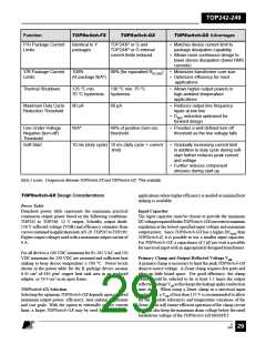
Standby Consumption
Frequency reduction can significantly reduce power loss at
lightornoload,especiallywhenaZenerclampisused. Forvery
low secondary power consumption use a TL431 regulator for
feedback control. Alternately, switching losses can be
significantly reduced by changing from 132 kHz in normal
operation to 66 kHz under light load conditions.
Heat Sinking
The tab of the Y package (TO-220) is internally electrically
tied to the SOURCE pin. To avoid circulating currents, a heat
sink attached to the tab should not be electrically tied to any
primary ground/source nodes on the PC board.
When using a P (DIP-8), G (SMD-8) or R (TO-263) package,
acopperareaunderneaththepackageconnectedtotheSOURCE
pins will act as an effective heat sink. On double sided boards
(Figure 49), top side and bottom side areas connected with vias
can be used to increase the effective heat sinking area.
TOPSwitch-GX Layout Considerations
AsTOPSwitch-GXhasadditionalpinsandoperatesatmuch
higher power levels compared to previous TOPSwitch
families, the following guidelines should be carefully
followed.
In addition, sufficient copper area should be provided at the
anode and cathode leads of the output diode(s) for heat sinking.
Primary Side Connections
Use a single point (Kelvin) connection at the negative terminal
of the input filter capacitor for TOPSwitch-GX source pin and
biaswindingreturn.Thisimprovessurgecapabilitiesbyreturning
surge currents from the bias winding directly to the input filter
capacitor.
In Figures 47, 48 and 49 a narrow trace is shown between the
output rectifier and output filter capacitor. This trace acts as a
thermal relief between the rectifier and filter capacitor to
prevent excessive heating of the capacitor.
Quick Design Checklist
The CONTROL pin bypass capacitor should be located as
close as possible to the SOURCE and CONTROL pins and its
SOURCE connection trace should not be shared by the main
MOSFET switching currents. All SOURCE pin referenced
components connected to the MULTI-FUNCTION, LINE-
SENSEorEXTERNALCURRENTLIMITpinsshouldalsobe
located closely between their respective pin and SOURCE.
OnceagaintheSOURCEconnectiontraceofthesecomponents
should not be shared by the main MOSFET switching currents.
It is very critical that SOURCE pin switching currents are
returned to the input capacitor negative terminal through a
seperate trace that is not shared by the components connected
to CONTROL, MULTI-FUNCTION, LINE-SENSE or
EXTERNAL CURRENT LIMIT pins. This is because the
SOURCE pin is also the controller ground reference pin.
As with any power supply design, all TOPSwitch-GX designs
should be verified on the bench to make sure that components
specifications are not exceeded under worst case conditions.
The following minimum set of tests is strongly recommended:
1. Maximum drain voltage – Verify that peak VDS does not
exceed675Vathighestinputvoltageandmaximumoverload
output power. Maximum overload output power occurs
when the output is overloaded to a level just before the
power supply goes into auto-restart (loss of regulation).
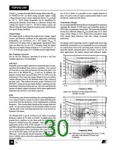
2. Maximumdraincurrent–Atmaximumambienttemperature,
maximum input voltage and maximum output load, verify
drain current waveforms at start-up for any signs of
transformer saturation and excessive leading edge current
spikes. TOPSwitch-GX has a leading edge blanking time of
220 ns to prevent premature termination of the on-cycle.
Verify that the leading edge current spike is below the
allowed current limit envelope (see Figure 52) for the drain
current waveform at the end of the 220 ns blanking period.
Any traces to the M, L or X pins should be kept as short as
possible and away from the DRAIN trace to prevent noise
coupling. LINE-SENSE resistor (R1 in figures 47-49) should
be located close to the M or L pin to minimize the trace length
on the M or L pin side.
3. Thermal check – At maximum output power, minimum
input voltage and maximum ambient temperature, verify
that temperature specifications are not exceeded for
TOPSwitch-GX, transformer, output diodes and output
capacitors. Enough thermal margin should be allowed for
In addition to the 47 µF CONTROL pin capacitor, a high
frequency bypass capacitor in parallel may be used for better
noise immunity. The feedback optocoupler output should also
be located close to the CONTROL and SOURCE pins of
TOPSwitch-GX.
E
7/01
August 8, 2000
31

 POWERINT [ Power Integrations ]