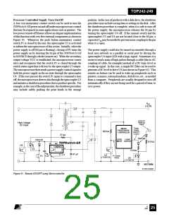
TOP242-249
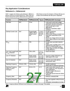
Function
TOPSwitch-FX
TOPSwitch-GX
TOPSwitch-GX Advantages
P/G Package Current
Limits
Identical to Y
packages
TOP243P or G and
TOP244P or G internal
current limits reduced
• Matches device current limit to
package dissipation capability
• Allows more continuous design to
lower device dissipation (lower RMS
currents)
Y/R Package Current
Limits
100%
(R package N/A*)
90% (for equivalent RDS (ON)
)
• Minimizes transformer core size
• Optimizes efficiency for most
applications
Thermal Shutdown
125 °C min.
70 °C hysteresis
130 °C min. 75 °C
hysteresis
• Allows higher output powers in
high ambient temperature
applications
Maximum Duty Cycle
Reduction Threshold
90 µA
60 µA
• Reduces output line frequency
ripple at low line
• DMAX reduction optimized for
forward design
Line Under-Voltage
Negative (turn-off)
Threshold
N/A*
40% of positive (turn-on)
threshold
• Provides a well defined turn-off
threshold as the line voltage falls
Soft-Start
10 ms (duty cycle) 10 ms (duty cycle + current
limit)
• Gradually increasing current limit
in addition to duty cycle during soft-
start further reduces peak current
and voltage
• Further reduces component
stresses during start up
Table 5 (cont). Comparison Between TOPSwitch-FX and TOPSwitch-GX. *Not available
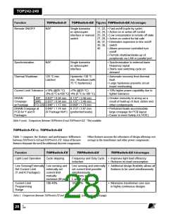
TOPSwitch-GX Design Considerations
applications where higher efficiency is needed or minimal heat
sinking is available.
Power Table
Datasheet power table represents the maximum practical
continuous output power based on the following conditions:
TOP242 to TOP246: 12 V output, Schottky output diode,
150 V reflected voltage (VOR) and efficiency estimates from
curvescontainedinapplicationnoteAN-29.TOP247toTOP249:
Higher output voltages used with a maximum output current of
6 A.
Input Capacitor
The input capacitor must be chosen to provide the minimum
DCvoltagerequiredfortheTOPSwitch-GXconvertertomaintain
regulation at the lowest specified input voltage and maximum
output power. Since TOPSwitch-GX has a higher DCMAX than
TOPSwitch-II, it is possible to use a smaller input capacitor.
For TOPSwitch-GX, a capacitance of 2 µF per watt is possible
for universal input with an appropriately designed transformer.
For all devices a 100 VDC minimum for 85-265 VAC and 250
VDC minimum for 230 VDC are assumed and sufficient heat
sinking to keep device temperature ≤ 100 °C. Power levels
shown in the power table for the R package device assume
6.45 cm2 of 610 g/m2 copper heat sink area in an enclosed
adapter, or 19.4 cm2 in an open frame.
Primary Clamp and Output Reflected Voltage VOR
A primary clamp is necessary to limit the peak TOPSwitch-GX
drain to source voltage. A Zener clamp requires few parts and
takes up little board space. For good efficiency, the clamp
Zener should be selected to be at least 1.5 times the output
reflectedvoltageVORasthiskeepstheleakagespikeconduction
time short. When using a Zener clamp in a universal input
application, a VOR of less than 135 V is recommended to allow
for the absolute tolerances and temperature variations of the
Zener. This will ensure efficient operation of the clamp circuit
and will also keep the maximum drain voltage below the rated
breakdown voltage of the TOPSwitch-GX MOSFET.
TOPSwitch-GX Selection
Selecting the optimum TOPSwitch-GX depends upon required
maximum output power, efficiency, heat sinking constraints
and cost goals. With the option to externally reduce current
limit, a larger TOPSwitch-GX may be used for lower power
E
7/01
August 8, 2000
29

 POWERINT [ Power Integrations ]