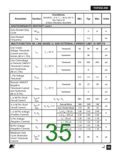
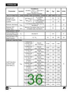
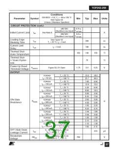
TOP242-250
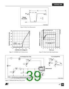
t
2
t
1
HV
90%
90%
t
t
DRAIN
VOLTAGE
1
2
D =
10%
0 V
PI-2039-033001
Figure 50. Duty Cycle Measurement.
t
(Blanking Time)
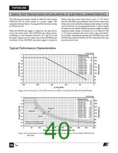
LEB
120
100
80
1.3
1.2
1.1
1.0
0.9
0.8
0.7
0.6
0.5
0.4
0.3
0.2
0.1
0
I
@ 85 VAC
INIT(MIN)
60
I
@ 265 VAC
INIT(MIN)
40
I
I
@ 25 °C
@ 25 °C
LIMIT(MAX)
LIMIT(MIN)
Dynamic
Impedance
1
=
Slope
20
0
0
2
4
6
8
10
0
1
2
3
4
5
6
7
8
CONTROL Pin Voltage (V)
Figure 51. CONTROL Pin I-V Characteristic.
Time (µs)
Figure 52. Drain Current Operating Envelope.
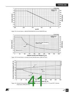
Y or R Package (X and L Pins)
P or G Package (M Pin)
0-100 kΩ
S1
470 Ω
5 W
0-100 kΩ
S5
5-50 V
M
5-50 V
0-60 kΩ
40 V
L
D
CONTROL
470 Ω
C
C
TOPSwitch-GX
S2
F
X
S
S4
0-15 V
S3
0-60 kΩ
47 µF
0.1 µF
NOTES: 1. This test circuit is not applicable for current limit or output characteristic measurements.
2. For P and G packages, short all SOURCE pins together.
PI-2631-081204
Figure 53. TOPSwitch-GX General Test Circuit.
M
12/04
39

 POWERINT [ Power Integrations ]