TOP242-250
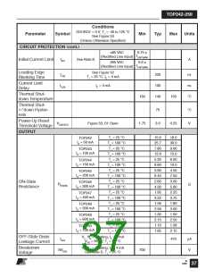
Parameter
Conditions
SOURCE = 0 V; TJ = -40 to 125 °C
See Figure 53
Symbol
Min
Typ
Max
Units
(Unless Otherwise Specified)
OUTPUT (cont.)
Rise Time
tR
tF
100
50
ns
ns
Measured in a Typical Flyback
Converter Application
Fall Time
SUPPLY VOLTAGE CHARACTERISTICS
DRAIN Supply
Voltage
See Note E
36
V
V
Shunt Regulator
Voltage
VC(SHUNT)
IC = 4 mA
5.60
5.85
±50
6.10
Shunt Regulator
Temperature Drift
ppm/°C
TOP242-245
1.0
1.2
1.3
1.6
2.2
2.4
2.5
3.2
Output MOSFET
Enabled
VX, VL, VM = 0 V
ICD1
TOP246-249
TOP250
3.65
Control Supply/
Discharge Current
mA
Output MOSFET
ICD2
Disabled
0.3
0.6
1.3
VX, VL, VM = 0 V
NOTES:
A. For specifications with negative values, a negative temperature coefficient corresponds to an increase in
magnitude with increasing temperature, and a positive temperature coefficient corresponds to a decrease in
magnitude with increasing temperature.
B. Guaranteed by characterization. Not tested in production.
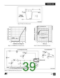
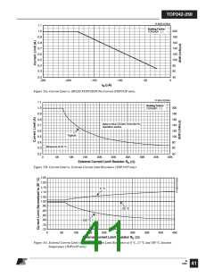
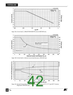
C. For externally adjusted current limit values, please refer to Figures 54b, 55b and 56b (Current Limit vs. External
Current Limit Resistance) in the Typical Performance Characteristics section. The tolerance specified is only valid
at full current limit.
D. Breakdown voltage may be checked against minimum BVDSS specification by ramping the DRAIN pin voltage up
to but not exceeding minimum BVDSS
.
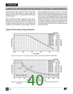
E. It is possible to start up and operate TOPSwitch-GX at DRAIN voltages well below 36 V. However, the CONTROL
pin charging current is reduced, which affects start-up time, auto-restart frequency, and auto-restart duty cycle.
Refer to Figure 68, the characteristic graph on CONTROL pin charge current (IC) vs. DRAIN voltage for low
voltage operation characteristics.
M
38 12/04

 POWERINT [ Power Integrations ]