TNY264/266-268
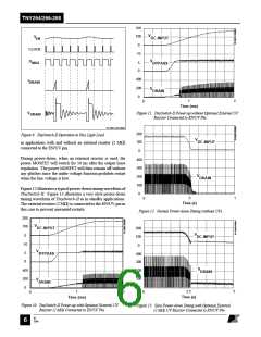
Capacitor C1 provides high frequency decoupling of the high
voltage DC supply, only necessary if there is a long trace length
from the DC bulk capacitors of the main supply. The line sense
resistors R2 and R3 sense the DC input voltage for line under-
voltage. When the AC is turned off, the under-voltage detect
feature of the TinySwitch-II prevents auto-restart glitches at the
outputcausedbytheslowdischargeoflargestoragecapacitance
in the main converter. This is achieved by preventing the
TinySwitch-II from switching when the input voltage goes
belowalevelneededtomaintainoutputregulation,andkeeping
it off until the input voltage goes above the under-voltage
threshold, when the AC is turned on again. With R2 and R3,
giving a combined value of 4 MΩ, the power up under-voltage
threshold is set at 200 VDC, slightly below the lowest required
operating DC input voltage, for start-up at 170 VAC, with
doubler. This feature saves several components needed to
implement the glitch-free turn-off compared with discrete or
TOPSwitch-II based designs. During turn-on the rectified DC
input voltage needs to exceed 200 V under-voltage threshold
for the power supply to start operation. But, once the power
supply is on it will continue to operate down to 140 V rectified
DC input voltage to provide the required hold up time for the
standby output.
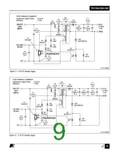
2.5 W CV/CC Cell-Phone Charger
As an example, Figure 14 shows a TNY264 based 5 V, 0.5 A,
cellular phone charger operating over a universal input range
(85-265VAC). Theinductor(L1)formsaπ-filterinconjunction
with C1 and C2. The resistor R1 damps resonances in the
inductor L1. Frequency jittering operation of TinySwitch-II
allowstheuseofasimpleπ-filterdescribedaboveincombination
with a single low value Y1-capacitor (C8) to meet worldwide
conducted EMI standards. The addition of a shield winding in
the transformer allows conducted EMI to be met even with the
output capacitively earthed (which is the worst case condition
forEMI). ThediodeD6, capacitorC3andresistorR2comprise
the clamp circuit, limiting the leakage inductance turn-off
voltage spike on the TinySwitch-II DRAIN pin to a safe value.
Theoutputvoltageisdeterminedbythesumoftheoptocoupler
U2 LED forward drop (~1 V), and Zener diode VR1 voltage.
Resistor R8 maintains a bias current through the Zener diode to
ensure it is operated close to the Zener test current.
A simple constant current circuit is implemented using the VBE
of transistor Q1 to sense the voltage across the current sense
resistor R4. When the drop across R4 exceeds the VBE of
transistor Q1, it turns on and takes over control of the loop by
driving the optocoupler LED. Resistor R6 assures sufficient
voltage to keep the control loop in operation down to zero volts
at the output. With the output shorted, the drop across R4 and
R6 (~1.2 V) is sufficient to keep the Q1 and LED circuit active.
Resistors R7 and R9 limit the forward current that could be
drawnthroughVR1byQ1underoutputshortcircuitconditions,
due to the voltage drop across R4 and R6.
The auxiliary primary side winding is rectified and filtered by
D2 and C2 to create a 12 V primary bias output voltage for the
main power supply primary controller. In addition, this voltage
is used to power the TinySwitch-II via R4. Although not
necessary for operation, supplying theTinySwitch-II externally
reducesthedevicequiescentdissipationbydisablingtheinternal
drainderivedcurrentsourcenormallyusedtokeeptheBYPASS
pin capacitor (C3) charged. An R4 value of 10 kΩ provides
600 µA into the BYPASS pin, which is slightly in excess of the
current consumption of TinySwitch-II. The excess current is
safely clamped by an on-chip active Zener diode to 6.3 V.
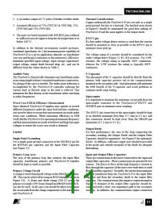
10 and 15 W PC Standby Circuits
Figures 15 and 16 show examples of circuits for PC standby
applications. They both provide two outputs: an isolated 5 V
anda12Vprimaryreferencedoutput.Thefirst,usingTNY266P,
provides 10W, and the second, using TNY267P, 15 W of
output power. Both operate from an input range of 140 to
375VDC, corresponding to a 230 VAC or 100/115 VAC with
doubler input. The designs take advantage of the line under-
voltage detect, auto-restart and higher switching frequency of
TinySwitch-II. Operationat132kHzallowstheuseofasmaller
and lower cost transformer core, EE16 for 10 W and EE22 for
15 W. The removal of pin 6 from the 8 pin DIP TinySwitch-II
packages provides a large creepage distance which improves
reliability in high pollution environments such as fan cooled
PC power supplies.
The secondary winding is rectified and filtered by D3 and C6.
For a 15W design an additional output capacitor, C7, is
required due to the larger secondary ripple currents compared
tothe10W PCstandbydesign. Theauto-restartfunctionlimits
output current during short circuit conditions, removing the
needtooverrateD3.SwitchingnoisefilteringisprovidedbyL1
and C8. The 5V output is sensed by U2 and VR1. R5 is used to
ensure that the Zener diode is biased at its test current.
TheZenerregulationmethodprovidessufficientaccuracy(typ.
3%). This is possible because TinySwitch-II limits the
dynamic range of the optocoupler LED current, allowing the
Zener diode to operate at near constant bias current.
B
7/01
8

 POWERINT [ Power Integrations ]