TNY264/266-268
Key Application Considerations
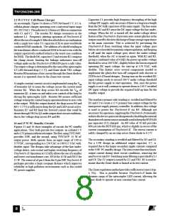
TinySwitch-II vs. TinySwitch
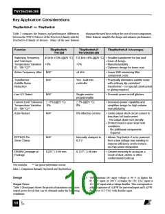
Table 2 compares the features and performance differences
between the TNY254 device of the TinySwitch family with the
TinySwitch-II family of devices. Many of the new features
eliminate the need for or reduce the cost of circuit components.
Other features simplify the design and enhance performance.
Function
TinySwitch
TinySwitch-II
TNY264/266-268
TinySwitch-II Advantages
TNY254
Switching Frequency
and Tolerance
44 kHz 10% (@25 °C) 132 kHz 6% (@25 °C) • Smaller transformer for low cost
• Ease of design
Temperature Variation +8%
+2%
• Manufacturability
(0 - 100 °C)**
• Optimum design for lower cost
Active Frequency Jitter
N/A*
N/A*
4 kHz
• Lower EMI minimizing filter
component costs
Transformer
Audible Noise
Reduction
Yes - built into
controller
• Practically eliminates audible noise
with ordinary dip varnished
transformer – no special construction
or gluing required
Line UV Detect
N/A*
Single resistor
programmable
• Prevents power on/off glitches
Current Limit Tolerance
Temperature Variation
(0 - 100 °C)**
11% (@25 °C)
-8%
7% (@25 °C)
0%
• Increases power capability and
simplifies design for high volume
manufacturing
Auto-Restart
N/A*
6% effective on-time
• Limits output short-circuit current to
less than full load current
- No output diode size penalty.
• Protects load in open loop fault
conditions
- No additional components
required
BYPASS Pin
Zener Clamp
N/A*
Internally clamped to
6.3 V
• Allows TinySwitch-II to be powered
from a low voltage bias winding to
improve efficiency and to reduce
on-chip power dissipation
DRAIN Creepage at
Package
0.037” / 0.94 mm
0.137” / 3.48 mm
• Greater immunity to arcing as a
result of dust, debris or other
contaminants build-up
*Not available.
** See typical performance curves.
Table 2. Comparison Between TinySwitch and TinySwitch-II.
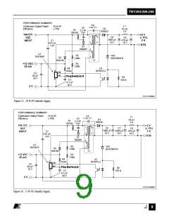
Design
1. The minimum DC input voltage is 90 V or higher for
85 VAC input, or 240 V or higher for 230 VAC input or
115 VAC input with a voltage doubler. This corresponds to
a filter capacitor of 3 µF/W for universal input and 1 µF/W
for 230 or 115 VAC with doubler input.
Output Power
Table 1 (front page) shows the practical maximum continuous
output power levels that can be obtained under the following
conditions:
B
7/01
10

 POWERINT [ Power Integrations ]