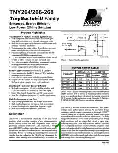
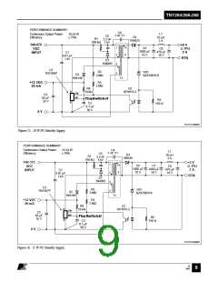
TNY264/266-268
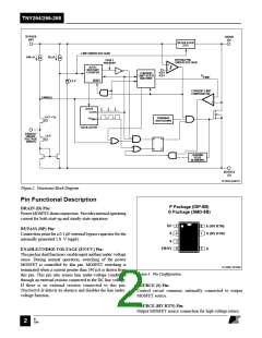
the SOURCE pin. The optocoupler LED is connected in series
withaZenerdiodeacrosstheDCoutputvoltagetoberegulated.
When the output voltage exceeds the target regulation voltage
level (optocoupler LED voltage drop plus Zener voltage), the
optocoupler LED will start to conduct, pulling the EN/UV pin
low. The Zener diode can be replaced by a TL431 reference
circuit for improved accuracy.
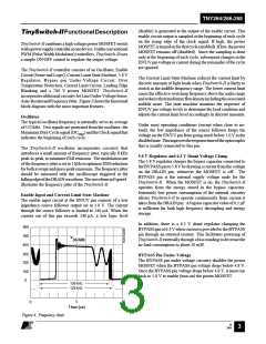
beginning of each clock cycle, it samples the EN/UV pin to
decide whether or not to implement a switch cycle, and based
on the sequence of samples over multiple cycles, it determines
the appropriate current limit. At high loads, when the EN/UV
pin is high (less than 240 µA out of the pin), a switching cycle
withthefullcurrentlimitoccurs. Atlighterloads, whenEN/UV
is high, a switching cycle with a reduced current limit occurs.
ON/OFF Operation with Current Limit State Machine
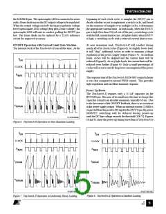
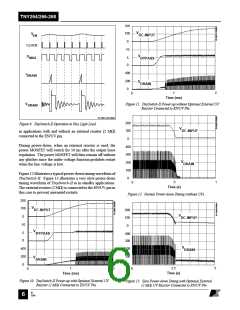
The internal clock of the TinySwitch-II runs all the time. At the
At near maximum load, TinySwitch-II will conduct during
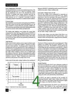
nearly all of its clock cycles (Figure 6). At slightly lower load,
it will “skip” additional cycles in order to maintain voltage
regulation at the power supply output (Figure 7). At medium
loads, cycles will be skipped and the current limit will be
reduced (Figure8). At very light loads, the current limit will be
reduced even further (Figure 9). Only a small percentage of
cycleswilloccurtosatisfythepowerconsumptionofthepower
supply.
V
EN
CLOCK
D
MAX
TheresponsetimeoftheTinySwitch-IION/OFFcontrolscheme
is very fast compared to normal PWM control. This provides
tight regulation and excellent transient response.
I
DRAIN
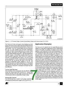
Power Up/Down
The TinySwitch-II requires only a 0.1 µF capacitor on the
BYPASS pin. Because of its small size, the time to charge this
capacitor is kept to an absolute minimum, typically 0.6 ms. Due
to the fast nature of the ON/OFF feedback, there is no overshoot
at the power supply output. When an external resistor (2 MΩ) is
connectedfromthepositiveDCinputtotheEN/UVpin,thepower
MOSFET switching will be delayed during power-up
until the DC line voltage exceeds the threshold (100 V). Figures
10 and 11 show the power-up timing waveform of TinySwitch-II
V
DRAIN
PI-2749-050301
Figure 6. TinySwitch-II Operation at Near Maximum Loading.
V
V
EN
EN
CLOCK
CLOCK
D
D
MAX
MAX
I
I
DRAIN
DRAIN
V
DRAIN
V
DRAIN
PI-2667-090700
PI-2377-091100
Figure 8. TinySwitch-II Operation at Medium Loading.
Figure 7. TinySwitch-II Operation at Moderately Heavy Loading.
B
7/01
5

 POWERINT [ Power Integrations ]