TNY253/254/255
REGULATOR
5.8 V
BYPASS
DRAIN
UNDERVOLTAGE
+
+
-
5.8 V
5.1 V
-
V
I
LIMIT
OSCILLATOR
CLOCK
50 μA
DC
THERMAL
MAX
SHUTDOWN
S
R
Q
Q
LEADING
EDGE
BLANKING
1.5 V + V
TH
SOURCE
ENABLE
PI-2197-061898
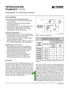
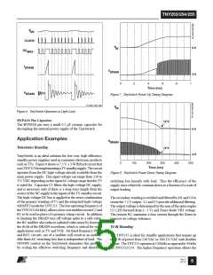
Figure 2. Functional Block Diagram.
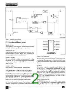
Pin Functional Description
DRAIN (D) Pin:
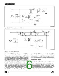
1
8
7
6
5
BYPASS
SOURCE
SOURCE
SOURCE
DRAIN
2
3
4
SOURCE
SOURCE
ENABLE
PowerꢀMOSFETꢀdrainꢀconnection.ꢀProvidesꢀinternalꢀoperatingꢀ
currentꢀforꢀbothꢀstart-upꢀandꢀsteady-stateꢀoperation.ꢀꢀ
BYPASS (BP) Pin:
Connectionꢀpointꢀforꢀanꢀexternalꢀbypassꢀcapacitorꢀforꢀtheꢀinter-
nallyꢀgeneratedꢀ5.8ꢀVꢀsupply.ꢀꢀBypassꢀpinꢀisꢀnotꢀintendedꢀforꢀ
sourcingꢀsupplyꢀcurrentꢀtoꢀexternalꢀcircuitry.
P Package (DIP-8)
G Package (SMD-8)
PI-2199-031501
Figure 3. Pin Configuration.
ENABLE (EN) Pin:
HystereticꢀOverꢀTemperatureꢀProtection,ꢀCurrentꢀLimitꢀcircuit,ꢀ
LeadingꢀEdgeꢀBlanking,ꢀandꢀaꢀ700ꢀVꢀpowerꢀMOSFET.ꢀꢀFigureꢀ
2ꢀshowsꢀaꢀfunctionalꢀblockꢀdiagramꢀwithꢀtheꢀmostꢀimportantꢀ
features.
TheꢀpowerꢀMOSFETꢀswitchingꢀcanꢀbeꢀterminatedꢀbyꢀpullingꢀ
thisꢀpinꢀlow.ꢀTheꢀI-Vꢀcharacteristicꢀofꢀthisꢀpinꢀisꢀequivalentꢀtoꢀ
aꢀvoltageꢀsourceꢀofꢀapproximatelyꢀ1.5ꢀVꢀwithꢀaꢀsourceꢀcurrentꢀ
clampꢀofꢀ50ꢀµA.ꢀ
Oscillator
SOURCE (S) Pin:
Theꢀoscillatorꢀfrequencyꢀisꢀinternallyꢀsetꢀatꢀ44ꢀkHzꢀ(130ꢀkHzꢀ
forꢀtheꢀTNY255).ꢀꢀTheꢀtwoꢀsignalsꢀofꢀinterestꢀareꢀtheꢀMaxi-
mumꢀDutyꢀCycleꢀsignalꢀ(DMAX)ꢀwhichꢀrunsꢀatꢀtypicallyꢀ67%ꢀ
dutyꢀcycleꢀandꢀtheꢀClockꢀsignalꢀthatꢀindicatesꢀtheꢀbeginningꢀofꢀ
eachꢀcycle.ꢀꢀWhenꢀcyclesꢀareꢀskippedꢀ(seeꢀbelow),ꢀtheꢀoscilla-
torꢀfrequencyꢀdoublesꢀ(exceptꢀforꢀTNY255ꢀwhichꢀremainsꢀatꢀ
130ꢀkHz).ꢀꢀThisꢀincreasesꢀtheꢀsamplingꢀrateꢀatꢀtheꢀENABLEꢀ
pinꢀforꢀfasterꢀloopꢀresponse.
PowerꢀMOSFETꢀsourceꢀconnection.ꢀꢀPrimaryꢀreturn.
TinySwitch Functional Description
TinySwitchꢀisꢀintendedꢀforꢀlowꢀpowerꢀoff-lineꢀapplications.ꢀꢀItꢀ
combinesꢀaꢀhigh-voltageꢀpowerꢀMOSFETꢀswitchꢀwithꢀaꢀpowerꢀ
supplyꢀcontrollerꢀinꢀoneꢀdevice.ꢀꢀUnlikeꢀaꢀconventionalꢀPWMꢀ
(Pulseꢀ Widthꢀ Modulator)ꢀ controller,ꢀ theꢀ TinySwitchꢀ usesꢀ aꢀ
simpleꢀON/OFFꢀcontrolꢀtoꢀregulateꢀtheꢀoutputꢀvoltage.
Enable (Sense and Logic)
TheꢀENABLEꢀpinꢀcircuitꢀhasꢀaꢀsourceꢀfollowerꢀinputꢀstageꢀsetꢀ
atꢀ1.5ꢀV.ꢀꢀTheꢀinputꢀcurrentꢀisꢀclampedꢀbyꢀaꢀcurrentꢀsourceꢀsetꢀ
atꢀ50ꢀµAꢀwithꢀ10ꢀµAꢀhysteresis.ꢀꢀTheꢀoutputꢀofꢀtheꢀenableꢀsenseꢀ
Theꢀ TinySwitchꢀ controllerꢀ consistsꢀ ofꢀ anꢀ Oscillator,ꢀ Enableꢀ
(SenseꢀandꢀLogic)ꢀcircuit,ꢀ5.8ꢀVꢀRegulator,ꢀUndervoltageꢀcircuit,ꢀ
Rev E
02/12
2

 POWERINT [ Power Integrations ]