TNY253/254/255
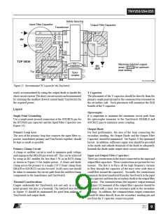
achieveꢀtheꢀappropriateꢀvalue.ꢀꢀR3ꢀisꢀaꢀbaseꢀcurrentꢀlimitingꢀ
resistor.ꢀꢀWhenꢀtheꢀdropꢀacrossꢀR4ꢀexceedsꢀtheꢀVBEꢀofꢀtransistorꢀ
Q1,ꢀitꢀturnsꢀonꢀandꢀtakesꢀoverꢀtheꢀcontrolꢀofꢀtheꢀloopꢀbyꢀdrivingꢀ
theꢀoptocouplerꢀLED.ꢀꢀR6ꢀdropsꢀanꢀadditionalꢀvoltageꢀtoꢀkeepꢀ
theꢀcontrolꢀloopꢀinꢀoperationꢀdownꢀtoꢀzeroꢀvoltsꢀonꢀtheꢀoutput.ꢀ
Withꢀtheꢀoutputꢀshorted,ꢀtheꢀdropꢀacrossꢀR4ꢀandꢀR6ꢀ(~ꢀ1.5ꢀV)ꢀisꢀ
sufficientꢀtoꢀkeepꢀtheꢀQ1ꢀandꢀLEDꢀcircuitꢀactive.ꢀꢀResistorsꢀR7ꢀ
andꢀR9ꢀlimitꢀtheꢀforwardꢀcurrentꢀthatꢀcouldꢀbeꢀdrawnꢀthroughꢀ
VR1ꢀbyꢀQ1ꢀunderꢀoutputꢀshort-circuitꢀconditions,ꢀdueꢀtoꢀtheꢀ
voltageꢀdropꢀacrossꢀR6ꢀandꢀR4.
Key Application Considerations
For the most up to date information visit our Web site
at: www.powerint.com
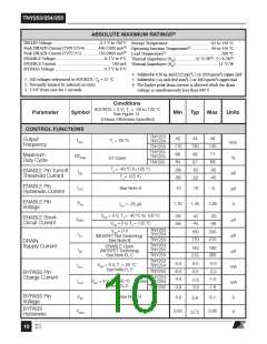
Design
Output Power Range
TheꢀpowerꢀlevelsꢀshownꢀinꢀtheꢀTinySwitchꢀSelectionꢀGuideꢀ
(Tableꢀ1)ꢀareꢀapproximate,ꢀrecommendedꢀoutputꢀpowerꢀrangesꢀ
thatꢀ willꢀ provideꢀ aꢀ costꢀ optimumꢀ designꢀ andꢀ areꢀ basedꢀ onꢀ
followingꢀassumptions:
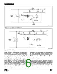
AC Adapter
Manyꢀconsumerꢀelectronicꢀproductsꢀutilizeꢀlowꢀpowerꢀ50/60ꢀHzꢀ
transformerꢀbasedꢀACꢀadapters.ꢀꢀTheꢀTinySwitchꢀcanꢀcostꢀef-
fectivelyꢀreplaceꢀtheseꢀlinearꢀadaptersꢀwithꢀaꢀsolutionꢀthatꢀisꢀ
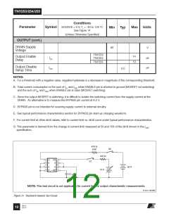
lighter,ꢀsmallerꢀandꢀmoreꢀenergyꢀefficientꢀ.ꢀꢀFigureꢀ12ꢀshowsꢀaꢀ
9ꢀV,ꢀ0.5ꢀWꢀACꢀadapterꢀcircuitꢀusingꢀtheꢀTNY253.ꢀꢀThisꢀcircuitꢀ
operatesꢀfromꢀaꢀ115ꢀVACꢀinput.ꢀꢀToꢀsaveꢀcost,ꢀthisꢀcircuitꢀrunsꢀ
withoutꢀanyꢀfeedback,ꢀinꢀdiscontinuousꢀconductionꢀmodeꢀtoꢀ
deliverꢀconstantꢀpowerꢀoutputꢀrelativelyꢀindependentꢀofꢀꢀin-
putꢀvoltage.ꢀꢀTheꢀoutputꢀvoltageꢀisꢀdeterminedꢀbyꢀtheꢀvoltageꢀ
dropꢀacrossꢀZenerꢀdiodeꢀVR1.ꢀꢀTheꢀprimaryꢀinductanceꢀofꢀtheꢀ
transformerꢀisꢀchosenꢀtoꢀdeliverꢀaꢀpowerꢀthatꢀisꢀinꢀexcessꢀofꢀtheꢀ
requiredꢀoutputꢀpowerꢀbyꢀatꢀleastꢀ50%ꢀtoꢀallowꢀforꢀcomponentꢀ
tolerancesꢀandꢀtoꢀmaintainꢀsomeꢀcurrentꢀthroughꢀtheꢀZenerꢀVR1ꢀ
atꢀfullꢀload.ꢀꢀAtꢀnoꢀload,ꢀallꢀofꢀtheꢀpowerꢀisꢀdeliveredꢀtoꢀtheꢀZenerꢀ
whichꢀshouldꢀbeꢀratedꢀandꢀheatꢀsinkedꢀaccordingly.ꢀꢀInꢀspiteꢀofꢀ
aꢀconstantꢀpowerꢀconsumptionꢀfromꢀtheꢀmainsꢀinput,ꢀthisꢀsolu-
tionꢀisꢀstillꢀsignificantlyꢀmoreꢀefficientꢀthanꢀlinearꢀadaptersꢀupꢀ
toꢀoutputꢀpowerꢀlevelsꢀofꢀapproximatelyꢀ1ꢀW.ꢀ
1.ꢀ TheꢀminimumꢀDCꢀinputꢀvoltageꢀisꢀ90ꢀVꢀorꢀhigherꢀforꢀ85ꢀVACꢀ
inputꢀorꢀ240ꢀVꢀorꢀhigherꢀforꢀ230ꢀVACꢀinputꢀorꢀ115ꢀVACꢀ
inputꢀwithꢀaꢀvoltageꢀdoubler.
2.ꢀ Theꢀ TinySwitchꢀ isꢀ notꢀ thermallyꢀ limitedꢀ -ꢀ theꢀ sourceꢀ
pinsꢀareꢀsolderedꢀtoꢀsufficientꢀcopperꢀareaꢀtoꢀkeepꢀtheꢀdieꢀ
temperatureꢀatꢀorꢀbelowꢀ100ꢀ°C.ꢀꢀThisꢀlimitationꢀdoesꢀnotꢀꢀ
usuallyꢀapplyꢀtoꢀTNY253ꢀandꢀTNY254.
TheꢀmaximumꢀpowerꢀcapabilityꢀofꢀaꢀTinySwitchꢀdependsꢀonꢀ
theꢀ thermalꢀ environment,ꢀ transformerꢀ coreꢀ sizeꢀ andꢀ designꢀ
(continuousꢀorꢀdiscontinuous),ꢀefficiencyꢀrequired,ꢀminimumꢀ
specifiedꢀinputꢀvoltage,ꢀinputꢀstorageꢀcapacitance,ꢀoutputꢀvolt-
age,ꢀoutputꢀdiodeꢀforwardꢀdrop,ꢀetc.,ꢀandꢀcanꢀbeꢀdifferentꢀfromꢀ
theꢀvaluesꢀshownꢀinꢀtheꢀselectionꢀguide.ꢀꢀ
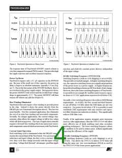
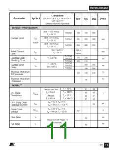
Audible Noise
Atꢀloadsꢀotherꢀthanꢀmaximumꢀload,ꢀtheꢀcycleꢀskippingꢀmodeꢀ
operationꢀusedꢀinꢀTinySwitchꢀcanꢀgenerateꢀaudioꢀfrequencyꢀ
componentsꢀinꢀtheꢀtransformer.ꢀꢀThisꢀcanꢀcauseꢀtheꢀtransformerꢀ
toꢀproduceꢀaudioꢀnoise.ꢀꢀTransformerꢀaudibleꢀnoiseꢀcanꢀbeꢀ
reducedꢀ byꢀ utilizingꢀ appropriateꢀ transformerꢀ constructionꢀ
techniquesꢀandꢀdecreasingꢀtheꢀpeakꢀfluxꢀdensity.ꢀꢀForꢀmoreꢀ
informationꢀ onꢀ audioꢀ suppressionꢀ techniques,ꢀ pleaseꢀ checkꢀ
theꢀ Applicationꢀ Notesꢀ sectionꢀ onꢀ ourꢀ Webꢀ siteꢀ atꢀ
www.powerint.com.ꢀꢀ
TheꢀACꢀinputꢀisꢀrectifiedꢀbyꢀdiodesꢀD1ꢀandꢀD2.ꢀꢀD2ꢀisꢀusedꢀtoꢀ
reduceꢀconductedꢀEMIꢀbyꢀonlyꢀallowingꢀnoiseꢀontoꢀtheꢀneutralꢀ
lineꢀduringꢀdiodeꢀconduction.ꢀꢀTheꢀrectifiedꢀACꢀisꢀthenꢀfilteredꢀ
byꢀcapacitorsꢀC1ꢀandꢀC2ꢀtoꢀgenerateꢀaꢀhigh-voltageꢀDCꢀbus,ꢀ
whichꢀisꢀappliedꢀtoꢀtheꢀseriesꢀcombinationꢀofꢀtheꢀprimaryꢀwind-
ingꢀofꢀT1ꢀandꢀtheꢀhigh-voltageꢀMOSFETꢀinsideꢀtheꢀTNY253.ꢀ
TheꢀresistorꢀR2ꢀalongꢀwithꢀcapacitorsꢀC1ꢀandꢀC2ꢀformꢀaꢀπ-filterꢀ
whichꢀisꢀsufficientꢀforꢀmeetingꢀEMIꢀconductedꢀemissionsꢀatꢀ
theseꢀpowerꢀlevels.ꢀꢀC5ꢀisꢀaꢀYꢀcapacitorꢀwhichꢀisꢀusedꢀtoꢀreduceꢀ
commonꢀmodeꢀEMI.ꢀꢀDueꢀtoꢀtheꢀ700ꢀVꢀratingꢀofꢀtheꢀTinySwitchꢀ
MOSFET,ꢀaꢀsimpleꢀcapacitiveꢀsnubberꢀ(C4)ꢀisꢀadequateꢀtoꢀlimitꢀ
theꢀleakageꢀinductanceꢀspikeꢀinꢀ115ꢀVACꢀapplications,ꢀatꢀlowꢀ
powerꢀlevels.ꢀꢀTheꢀsecondaryꢀwindingꢀisꢀrectifiedꢀandꢀfilteredꢀ
byꢀD3ꢀandꢀC6.
CeramicꢀcapacitorsꢀthatꢀuseꢀdielectricsꢀsuchꢀasꢀZ5U,ꢀwhenꢀusedꢀ
inꢀclampꢀandꢀsnubberꢀcircuits,ꢀcanꢀalsoꢀgenerateꢀaudioꢀnoiseꢀ
dueꢀtoꢀelectrostrictionꢀandꢀpiezo-electricꢀeffects.ꢀꢀIfꢀthisꢀisꢀtheꢀ
case,ꢀreplacingꢀthemꢀwithꢀaꢀcapacitorꢀhavingꢀaꢀdifferentꢀtypeꢀ
ofꢀdielectricꢀisꢀtheꢀsimplestꢀsolution.ꢀꢀPolyesterꢀfilmꢀcapacitorꢀ
isꢀaꢀꢀgoodꢀalternative.
Short-Circuit Current
TheꢀTinySwitchꢀdoesꢀnotꢀhaveꢀanꢀauto-restartꢀfeature.ꢀꢀAsꢀaꢀ
result,ꢀTinySwitchꢀwillꢀcontinueꢀtoꢀdeliverꢀpowerꢀtoꢀtheꢀloadꢀ
duringꢀoutputꢀshort-circuitꢀconditions.ꢀꢀInꢀtheꢀworstꢀcase,ꢀpeakꢀ
short-circuitꢀcurrentꢀisꢀequalꢀtoꢀtheꢀprimaryꢀcurrentꢀlimitꢀ(ILIMIT)ꢀ
multipliedꢀꢀbyꢀtheꢀturnsꢀratioꢀofꢀtheꢀtransformerꢀ(Np/Ns).ꢀꢀInꢀ
aꢀtypicalꢀdesignꢀtheꢀaverageꢀcurrentꢀisꢀ25ꢀtoꢀ50%ꢀlowerꢀthanꢀ
thisꢀpeakꢀvalue.ꢀꢀAtꢀtheꢀpowerꢀlevelsꢀofꢀTinySwitchꢀthisꢀisꢀ
Rev E
02/12
8

 POWERINT [ Power Integrations ]