TNY253/254/255
Safety Spacing
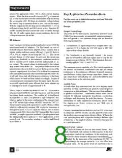
Transformer
Input Filter Capacitor
Output Filter Capacitor
+
HV
SEC
PRI
–
S
D
TOP VIEW
Y1-
Maximize hatched copper
Capacitor
DC
OUT
–
+
TinySwitch
areas (
) for optimum
heat sinking
CBP
Opto-
coupler
S
BP
EN
PI-2176-071398
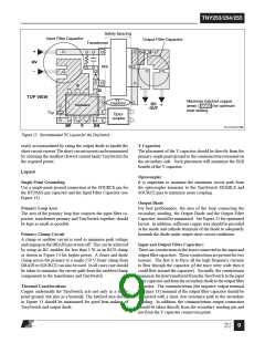
Figure 13. Recommended PC Layout for the TinySwitch.
easilyꢀaccommodatedꢀbyꢀratingꢀtheꢀoutputꢀdiodeꢀtoꢀhandleꢀtheꢀ
short-circuitꢀcurrent.ꢀTheꢀshort-circuitꢀcurrentꢀcanꢀbeꢀminimizedꢀ
byꢀchoosingꢀtheꢀsmallestꢀ(lowestꢀcurrentꢀlimit)ꢀTinySwitchꢀforꢀ
theꢀrequiredꢀpower.
Y Capacitor
TheꢀplacementꢀofꢀtheꢀYꢀcapacitorꢀshouldꢀbeꢀdirectlyꢀfromꢀtheꢀ
primaryꢀsingleꢀpointꢀgroundꢀtoꢀtheꢀcommon/returnꢀterminalꢀonꢀ
theꢀsecondaryꢀside.ꢀꢀSuchꢀplacementꢀwillꢀmaximizeꢀtheꢀEMIꢀ
benefitꢀofꢀtheꢀYꢀcapacitor.
Layout
Optocoupler
Single Point Grounding
Itꢀ isꢀ importantꢀ toꢀ maintainꢀ theꢀ minimumꢀ circuitꢀ pathꢀ fromꢀ
theꢀoptocouplerꢀtransistorꢀtoꢀtheꢀTinySwitchꢀENABLEꢀandꢀ
SOURCEꢀpinsꢀtoꢀminimizeꢀnoiseꢀcoupling.
UseꢀaꢀsingleꢀpointꢀgroundꢀconnectionꢀatꢀtheꢀSOURCEꢀpinꢀforꢀ
theꢀBYPASSꢀpinꢀcapacitorꢀandꢀtheꢀInputꢀFilterꢀCapacitorꢀ(seeꢀ
Figureꢀ13).
Output Diodeꢀ
Primary Loop Area
Forꢀ bestꢀ performance,ꢀ theꢀ areaꢀ ofꢀ theꢀ loopꢀ connectingꢀ theꢀ
secondaryꢀwinding,ꢀtheꢀOutputꢀDiodeꢀandꢀtheꢀOutputꢀFilterꢀ
Capacitor,ꢀshouldꢀbeꢀminimized.ꢀꢀSeeꢀFigureꢀ13ꢀforꢀoptimizedꢀ
layout.ꢀꢀInꢀaddition,ꢀsufficientꢀcopperꢀareaꢀshouldꢀbeꢀprovidedꢀ
atꢀtheꢀanodeꢀandꢀcathodeꢀterminalsꢀofꢀtheꢀdiodeꢀtoꢀadequatelyꢀ
heatsinkꢀtheꢀdiodeꢀunderꢀoutputꢀshort-circuitꢀconditions.ꢀ
Theꢀareaꢀofꢀtheꢀprimaryꢀloopꢀthatꢀconnectsꢀtheꢀinputꢀfilterꢀca-
pacitor,ꢀtransformerꢀprimaryꢀandꢀTinySwitchꢀtogether,ꢀshouldꢀ
beꢀkeptꢀasꢀsmallꢀasꢀpossible.ꢀ
Primary Clamp Circuit
Aꢀclampꢀorꢀsnubberꢀcircuitꢀisꢀusedꢀtoꢀminimizeꢀpeakꢀvoltageꢀ
andꢀringingꢀonꢀtheꢀDRAINꢀpinꢀatꢀturn-off.ꢀꢀThisꢀcanꢀbeꢀachievedꢀ
byꢀusingꢀanꢀRCꢀsnubberꢀforꢀlessꢀthanꢀ3ꢀWꢀorꢀanꢀRCDꢀclampꢀ
asꢀshownꢀinꢀFigureꢀ13ꢀforꢀhigherꢀpower.ꢀꢀAꢀZenerꢀandꢀdiodeꢀ
clampꢀacrossꢀtheꢀprimaryꢀorꢀaꢀsingleꢀ550ꢀVꢀZenerꢀclampꢀfromꢀ
DRAINꢀtoꢀSOURCEꢀcanꢀalsoꢀbeꢀused.ꢀꢀInꢀallꢀcasesꢀcareꢀshouldꢀ
beꢀtakenꢀtoꢀminimizeꢀtheꢀcircuitꢀpathꢀfromꢀtheꢀsnubber/clampꢀ
componentsꢀtoꢀtheꢀtransformerꢀandꢀTinySwitch.
Input and Output Filter Capacitors
Thereꢀareꢀconstrictionsꢀinꢀtheꢀtracesꢀconnectedꢀtoꢀtheꢀinputꢀandꢀ
outputꢀfilterꢀcapacitors.ꢀꢀTheseꢀconstrictionsꢀareꢀpresentꢀforꢀtwoꢀ
reasons.ꢀꢀTheꢀfirstꢀisꢀtoꢀforceꢀallꢀtheꢀhighꢀfrequencyꢀcurrentsꢀ
toꢀflowꢀthroughꢀtheꢀcapacitorꢀ(ifꢀtheꢀtraceꢀwereꢀwideꢀthenꢀitꢀ
couldꢀflowꢀaroundꢀtheꢀcapacitor).ꢀꢀSecondly,ꢀtheꢀconstrictionsꢀ
minimizeꢀtheꢀheatꢀtransferredꢀfromꢀtheꢀTinySwitchꢀtoꢀtheꢀinputꢀ
filterꢀcapacitorꢀandꢀfromꢀtheꢀsecondaryꢀdiodeꢀtoꢀtheꢀoutputꢀfilterꢀ
capacitor.ꢀꢀTheꢀcommon/returnꢀ(theꢀnegativeꢀoutputꢀterminalꢀ
inꢀFigureꢀ13)ꢀterminalꢀofꢀtheꢀoutputꢀfilterꢀcapacitorꢀshouldꢀbeꢀ
connectedꢀwithꢀaꢀshort,ꢀlowꢀresistanceꢀpathꢀtoꢀtheꢀsecondaryꢀ
winding.ꢀꢀInꢀaddition,ꢀtheꢀcommon/returnꢀoutputꢀconnectionꢀ
shouldꢀbeꢀtakenꢀdirectlyꢀfromꢀtheꢀsecondaryꢀwindingꢀpinꢀandꢀ
notꢀfromꢀtheꢀYꢀcapacitorꢀconnectionꢀpoint.
Thermal Considerations
CopperꢀunderneathꢀtheꢀTinySwitchꢀactsꢀnotꢀonlyꢀasꢀaꢀsingleꢀ
pointꢀground,ꢀbutꢀalsoꢀasꢀaꢀheatsink.ꢀTheꢀhatchedꢀareaꢀshownꢀ
inꢀFigureꢀ13ꢀshouldꢀbeꢀmaximizedꢀforꢀgoodꢀheat-sinkingꢀofꢀ
TinySwitchꢀandꢀoutputꢀdiode.ꢀꢀ
Rev E
02/12
9

 POWERINT [ Power Integrations ]