RELEASED
PM7350 S/UNI DUPLEX
DATA SHEET
PMC-1980581
ISSUE 8
DUAL SERIAL LINK PHY MULTIPLEXER
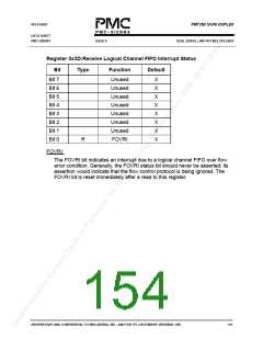
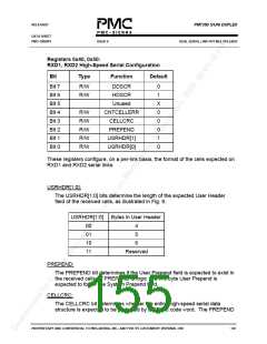
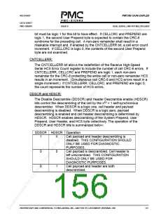
Register 0x3C: Receive Logical Channel FIFO Control
Bit
Type
Function
Default
Bit 7
Bit 6
Bit 5
Bit 4
Bit 3
Bit 2
Bit 1
Bit 0
Unused
Unused
Unused
Unused
Unused
Unused
FOVRE
FIFORST
X
X
X
X
X
X
0
R/W
R/W
0
FIFORST:
The FIFORST bit is used to reset all logical channel FIFOs for the receive
link. When FIFORST is set to logic 0, the FIFO channels operate normally.
When FIFORST is set to logic 1, all the FIFOs are immediately emptied and
ignore writes from the active LVDS link. While the FIFO is reset the flow
control information sent to the far end (via the LVDS link) indicates “buffer full
or unavailable” for all channels. The FIFOs remain empty and continue to
ignore writes until logic 0 is written to FIFORST.
To prevent unstable behavior during cell format configuration, FIFORST
should be left asserted while changing the cell format or length.
If a cell is being transferred from the SCIPHY/Any-PHY output port or from
the Clocked Serial Data interface when a reset of the FIFO occurs the cell will
be corrupted.
When using the SCI-PHY/Any-PHY output port as a bus slave, the bus
master need not have started the cell transfer (in response to the asserted
OCA from the S/UNI-DUPLEX) for cell corruption to occur. The S/UNI-
DUPLEX uses a partial look ahead buffer that cannot be reset by the Receive
Logical Channel FIFO reset. Even if the bus master suspends cell transfers
during the time when the Receive Logical Channel FIFO is reset, the next cell
read from the S/UNI-DUPLEX will be corrupted if there was a cell wainting for
transfer when the FIFO reset occurred. The simplest approach is to allow the
bus master to continue normal operation during a FIFO reset. If required, the
bus master can discard any cells received from that link after it is reset.
PROPRIETARY AND CONFIDENTIAL TO PMC-SIERRA, INC., AND FOR ITS CUSTOMERS’ INTERNAL USE
137

 PMC [ PMC-SIERRA, INC ]