S/UNI-IMA-4 Telecom Standard Product Data Sheet
Released
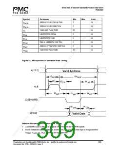
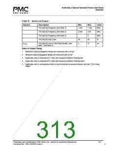
Symbol
tS
Parameter
Address to Latch Set-up Time
Min
5
Max
Units
ns
ALW
Address to Latch Hold Time
Valid Latch Pulse Width
Latch to Write Set-up
5
ns
ns
ns
ns
ns
ns
ns
tH
ALW
L
20
0
tV
tS
LW
Latch to Write Hold
5
tH
tH
tH
LW
DW
AW
WR
Data to Valid Write Hold Time
Address to Valid Write Hold Time
Valid Write Pulse Width
5
5
20
tV
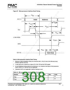
Figure 52 Microprocessor Interface Write Timing
A[10:1]
Valid Address
tS
tH
ALW
ALW
tV
tS
tH
LW
L
LW
ALE
(CSB+WRB)
D[15:0]
tS
tV
tS
tH
AW
AW
WR
tH
DW
DW
Valid Data
Notes on Microprocessor Interface Write Timing:
1. A valid write cycle is defined as a logical OR of the CSB and the WRB signals.
2. In non-multiplexed address/data bus architectures, ALE should be held high so that parameters
tS , tS , tV , tS and tH are not applicable.
ALW ALW LW LW
L
Proprietary and Confidential to PMC-Sierra, Inc., and for its customers’ internal use.
Document No.: PMC-2020889, Issue 2
309

 PMC [ PMC-SIERRA, INC ]