S/UNI-IMA-4 Telecom Standard Product Data Sheet
Released
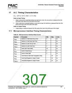
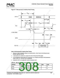
Figure 51 Microprocessor Interface Read Timing
tS
AR
A[10:1]
ALE
Valid
Address
tH
AR
tS
ALR
tV
tH
L
ALR
tH
tS
LR
LR
(CSB+RDB)
INTB
tZ
INTH
tZ
tP
RD
RD
D[15:0]
Valid Data
Notes on Microprocessor Interface Read Timing:
1. Maximum output propagation delays are measured with a 100 pF load on the Microprocessor
Interface data bus (D[15:0]).
2. A valid read cycle is defined as a logical OR of the CSB and the RDB signals.
3. In non-multiplexed address/data bus architectures, ALE should be held high so that parameters
tSALR, tHALR, tVL, and tSLR are not applicable.
4. Parameter tHAR is not applicable if address latching is used.
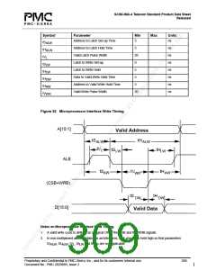
Table 44 Microprocessor Interface Write Access
Symbol
Parameter
Address to Valid Write Set-up Time
Min
5
Max
Units
ns
tS
AW
DW
Data to Valid Write Set-up Time
10
ns
tS
Proprietary and Confidential to PMC-Sierra, Inc., and for its customers’ internal use.
Document No.: PMC-2020889, Issue 2
308

 PMC [ PMC-SIERRA, INC ]