S/UNI®-ATLAS-3200 Telecom Standard Product Data Sheet
Preliminary
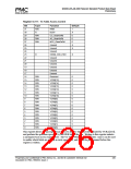
SA[16:0]
This register holds the SRAM Address to be used for the Microprocessor initiated accesses.
SA[16:0] map directly to device pins SADDR[16:0].
Search/Linkage
This bit indicates whether the operation is to address a Searching row or a Linkage row. The
access is to a Search row if this bit is logic 0, and to a Linkage row if this bit is logic 1. This
bit maps directly to device pin SADDR[17].
BUSY
The BUSY bit is high while a Microprocessor initiated access request to the SRAM is
pending. This register should be polled until the BUSY bit goes low before another
microprocessor access request is initiated. A microprocessor access request is typically
completed within 22 SYSCLK cycles. The maximum possible latency for a read is 40 cycles,
and for a write is 90 cycles. If the STANDBY bit in the S/UNI-ATLAS-3200 Master
Configuration register is a logic 1, the typical access time is reduced to less than 7 SYSCLK
cycles.
RWB
The RWB bit selects the operation to be performed on the addressed VC Table: when RWB is
set to a logic 1, a read from the SRAM is requested; when RWB is set to a logic 0, a write to
the SRAM is requested.
Proprietary and Confidential to PMC-Sierra, Inc., and for its Customers’ Internal Use
Document ID: PMC-1990553, Issue 4
222

 PMC [ PMC-SIERRA, INC ]