S/UNI®-ATLAS-3200 Telecom Standard Product Data Sheet
Preliminary
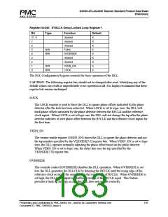
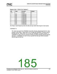
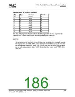
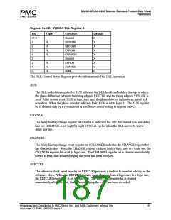
Register 0x040: SYSCLK Delay Locked Loop Register 1
Bit
31: 8
Type
Function
Unused
Unused
Unused
FUNC
OVERRIDE
Unused
Unused
VERN_EN
LOCK
Default
X
X
X
0
7
6
5
4
3
2
1
0
R/W
R/W
0
X
X
0
R/W
R/W
0
The DLL Configuration Register controls the basic operation of the DLL.
CAUTION: The following register bits should not be changed after reset. Modifying any of the
default values can result in unpredictable or no operation at all. It is highly recommend that these
register bits remain unchanged.
LOCK
The LOCK register is used to force the DLL to ignore phase offsets indicated by the phase
detector after the lock has been achieved. When LOCK is set to logic zero, the DLL will
track phase offsets measured by the phase detector between the RFCLK and the reference
clock inputs. When LOCK is set to logic one, the DLL will not change the tap after the phase
detector indicates of zero phase offset between the RFCLK and the reference clock inputs for
the first time.
VERN_EN
The vernier enable register (VERN_EN) forces the DLL to ignore the phase detector and use
the tap number specified by the VERNIER[7:0] register bits. When VERN_EN is set to logic
zero, the DLL operates normally adjusting the phase offset based on the phase detector.
When VERN_EN is set to logic one, the delay line uses the tap specified by the
VERNIER[7:0] register bits.
OVERRIDE
The override control (OVERRIDE) disables the DLL operation. When OVERRIDE is set
low, the DLL generates the DLLCLK by delaying the RFCLK until the rising edge of the
reference clock occurs at the same time as the rising edge of RFCLK. When OVERRIDE is
set high, the DLLCLK output is a buffered version of the RFCLK input. This feature
provides a back-up strategy in case the DLL does not operate correctly.
Proprietary and Confidential to PMC-Sierra, Inc., and for its Customers’ Internal Use
Document ID: PMC-1990553, Issue 4
183

 PMC [ PMC-SIERRA, INC ]