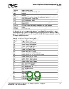
S/UNI®-8x155 ASSP Telecom Standard Product Data Sheet
Released
Address
1001
Register Description
S/UNI-8x155 DCC Interface Configuration
1002
Reserved
1003
Reserved
1004-10FF
1100
System and APS Interface Configuration and Status Registers
CSPI Clock Synthesis Configuration
1101
CSPI Clock Synthesis Status
1102
CSPI Reserved
1103
CSPI Reserved
1104-11FF
1200-1FFF
2000-3FFF
APS Cross Connect and Aligner Configuration and Status Registers
Unused
Reserved for Test
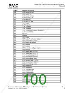
As shown by the top level register map in Table 7, each channel is represented by a repeat
addressable structure. Table 8 describes every normal mode register for a channel’s address
space. The channel offset is shown for channel #0 with all other channels similarly located by
the address spaces listed above.
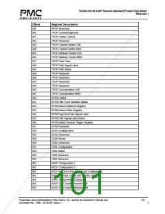
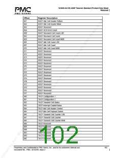
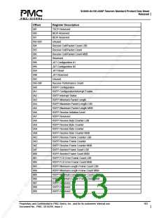
Table 8 Per Channel Register Memory Map
Offset
004
005
006
007
008
009
00A
00B
00C
00D
00E
00F
010
011
012
013
014
015
016
017
018
019
Register Description
Channel Master Configuration #1
Channel Master Configuration #2
Channel Reset/Interrupt Status #1
Channel Interrupt Status #2
Channel Auto Line RDI Control
Channel Auto Path RDI Control
Channel Auto Enhanced Path RDI Control
Channel Receive RDI and Enhanced RDI Control
Channel Receive Line AIS Control
Channel Receive Path AIS Control
Channel Receive Alarm Control #1
Channel Receive Alarm Control #2
RSOP Control/Interrupt Enable
RSOP Status/Interrupt Status
RSOP Section BIP-8 LSB
RSOP Section BIP-8 MSB
TSOP Control
TSOP Diagnostic
TSOP Reserved
TSOP Reserved
RLOP Control/Status
RLOP Interrupt Enable/Interrupt Status
Proprietary and Confidential to PMC-Sierra, Inc., and for its customers’ internal use.
Document No.: PMC- 2010299, Issue 2
99

 PMC [ PMC-SIERRA, INC ]