S/UNI®-8x155 ASSP Telecom Standard Product Data Sheet
Released
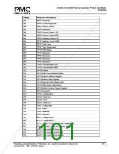
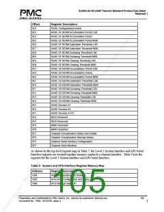
Offset
0E2
0E3
0E4
0E5
0E6
0E7
0E8
0E9
0EA
0EB
0EC
0ED
0EE
0EF
0F0
0F1
0F2
0F3
0F4
0F5
0F6
0F7
0F8
0F9
0FA
0FB
0FC
0FD
0FE
0FF
Register Description
RASE Configuration/Control
RASE SF BERM Accumulation Period LSB
RASE SF BERM Accumulation Period
RASE SF BERM Accumulation Period MSB
RASE SF BERM Saturation Threshold LSB
RASE SF BERM Saturation Threshold MSB
RASE SF BERM Declaring Threshold LSB
RASE SF BERM Declaring Threshold MSB
RASE SF BERM Clearing Threshold LSB
RASE SF BERM Clearing Threshold MSB
RASE SD BERM Accumulation Period LSB
RASE SD BERM Accumulation Period
RASE SD BERM Accumulation Period MSB
RASE SD BERM Saturation Threshold LSB
RASE SD BERM Saturation Threshold MSB
RASE SD BERM Declaring Threshold LSB
RASE SD BERM Declaring Threshold MSB
RASE SD BERM Clearing Threshold LSB
RASE SD BERM Clearing Threshold MSB
RASE Receive K1
RASE Receive K2
RASE Receive Z1/S1
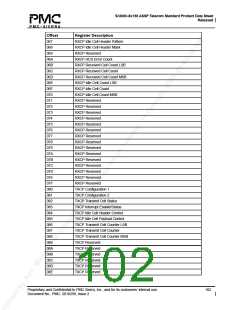
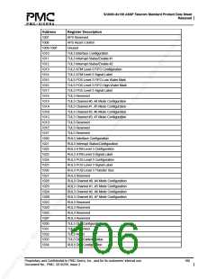
BIDX Reserved
BIDX Reserved
BIMX Reserved
BIMX Reserved
Channel Concatenation Status and Enable
Channel Concatenation Interrupt Status
Channel Serial Interface Configuration
Channel Clock Monitors
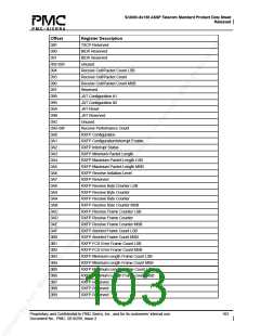
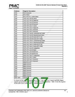
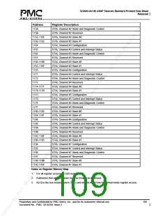
As shown by the top level register map in Table 7, the Level 3 System Interface and APS Serial
Interface registers are located together memory similar to a channel interface. Table 9 lists the
registers for the Level 3 System interface and APS Serial Interface.
Table 9 System and APS Interface Register Memory Map
Address
1004
1005
Register Description
APS Configuration and Status
APS FIFO Configuration and Status
APS Interrupt Status #1
1006
Proprietary and Confidential to PMC-Sierra, Inc., and for its customers’ internal use.
Document No.: PMC- 2010299, Issue 2
105

 PMC [ PMC-SIERRA, INC ]