Pm49FL002 / 004
PMC
GENERAL DESCRIPTION
The Pm49FL002/004 are 2 Mbit/4 Mbit 3.3 Volt-only Flash Memories used as BIOS in PCs and Notebooks. These
devices are designed to use a single low voltage, ranging from 3.0 Volt to 3.6 Volt, power supply to perform in-
system or off-system read, erase and program operations. The 12.0 Volt VPP power supply are not required for the
program and erase operations of devices. The devices conform to Intel® Low Pin Count (LPC) Interface specification
revision 1.1 and also read-compatible with Intel 82802 Firmware Hub (FWH) for most PC and Notebook applica-
tions. The Pm49FL002/004 support two configurable interfaces: In-system hardware interface which can automatic
detect the FWH or LPC memory cycle for in-system read and write operations, and Address/Address Multiplexed
(A/A Mux) interface for fast manufacturing on EPROM Programmers. These devices are designed to work with both
Intel Family chipset and Non-Intel Family Chipset platforms, it will provide PC and Notebook manufacturers great
flexibility and simplicity for design, procurement, and material inventory.
The memory array of Pm49FL002 is divided into uniform 4 Kbyte sectors, or uniform 16 Kbytes blocks (sector
group - consists of four adjecent sectors). The memory array of Pm49FL004 is divided into uniform 4 Kbyte sectors,
or uniform 64 Kbyte blocks (sector group - consists of sixteen adjecent sectors). The sector or block erase feature
allows users to flexibly erase a memory area as small as 4 Kbyte or as large as 64 Kbyte by one single erase
operation without affecting the data in others. The chip erase feature allows the whole memory to be erased in one
single erase operation. The devices can be programmed on a byte-by-byte basis after performing the erase opera-
tion.
The program operation of Pm49FL002/004 is executed by issuing the program command code into command
register. The internal control logic automatically handles the programming voltage ramp-up and timing. The erase
operation of the devices is executed by issuing the sector, block, or chip erase command code into command
register. The internal control logic automatically handles the erase voltage ramp-up and timing. The preprogramming
on the array which has not been programmed is not required before an erase operation. The devices offer Data#
Polling and Toggle Bit functions in FWH/LPC and A/A Mux modes, the progress or completion of program and
erase operations can be detected by reading the Data# Polling on I/O7 or Toggle Bit on I/O6.
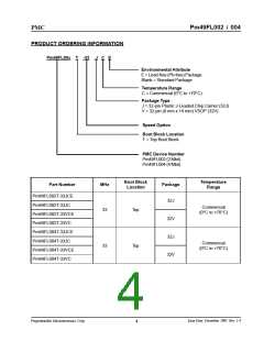
The Pm49FL002 has a 16 Kbyte top boot block which can be used to store user security data and code. The
Pm49FL004 has a 64 Kbyte top boot block. The boot block can be write protected by a hardware method controlled
by the TBL# pin or a register-based protection turned on/off by the Block Locking Registers (FWH mode only). The
rest of blocks except boot block in the devices also can be write protected by WP# pin or Block Locking Registers
(FWH mode only).
The Pm49FL002/004 are manufactured on PMC’s advanced nonvolatile technology, P-FLASH™. The devices are
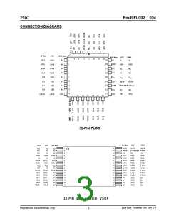
offered in 32-pin VSOP and PLCC packages with optional environmental friendly lead-free package.
Issue Date: December, 2003 Rev: 1.4
Programmable Microelectronics Corp.
2

 PMC [ PMC-SIERRA, INC ]