February, 2007
JTAG Interface Signals
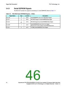
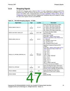
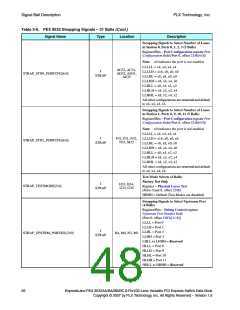
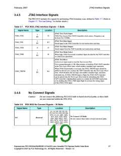
3.4.5
JTAG Interface Signals
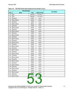
The PEX 8532 includes five signals for performing JTAG boundary scan, defined in Table 3-7. (Refer to
Chapter 17, “Test and Debug,” for further details.)
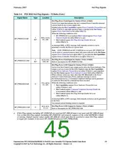
Table 3-7. PEX 8532 JTAG Interface Signals – 5 Balls
Signal Name
Type
Location
Description
JTAG Test Clock Input
JTAG Test Access Port (TAP) Controller clock source. Frequency can
be from 0 to 10 MHz.
I
PU
JTAG_TCK
J2
JTAG Test Data Input
Serial input to the TAP Controller for test instructions and data.
I
PU
JTAG_TDI
JTAG_TDO
K3
J3
JTAG Test Data Output
Serial output from the TAP Controller test instructions and data.
O
JTAG Test Mode Select
When high, JTAG Test mode is enabled. Input decoded by the TAP Controller
to control test operations.
I
PU
JTAG_TMS
J4
JTAG Test Reset
Active-Low input used to reset the Test Access Port.
Tie to ground through a 1.5K-Ohm resistor, to hold the JTAG TAP Controller
in the Test-Logic-Reset state, which enables standard logic operation.
When JTAG functionality is not used, the JTAG_TRST# input should be
pulled or driven Low, to place the TAP Controller into the Test-Logic-Reset
state, which disables the test logic and enables standard logic operation.
I
PU
JTAG_TRST#
K4
Alternatively, if JTAG_TRST# input is High, the JTAG TAP Controller
can be placed into the Test-Logic-Reset state by initializing the JTAG
TAP Controller’s Instruction register to contain the IDCODE instruction,
or by holding the JTAG_TMS input High for at least five rising edges
of the JTAG_TCK input.
3.4.6
No Connect Signals
Caution:
Do not connect the following PEX 8532 balls to board electrical paths, as these balls
are not connected within the PEX 8532.
Table 3-8. PEX 8532 No Connect Signals – 35 Balls
Signal Name
Type
Location
Description
A1, A2, B1, B2, D3, E3,
F3, G2, G3, G32, H3, H4,
H31, L3, L4, AB3, AB4,
AC3, AC4, AD3, AD4,
AE3, AE4, AE31, AF3,
AF4, AF31, AF32, AG3,
AH3, AH32, AN1, AN2,
AP1, AP2
No Connect (35 Balls)
Do not connect these balls to board electrical paths.
N/C
Reserved
ExpressLane PEX 8532AA/BA/BB/BC 8-Port/32-Lane Versatile PCI Express Switch Data Book
Copyright © 2007 by PLX Technology, Inc. All Rights Reserved – Version 1.6
27

 PLX [ PLX TECHNOLOGY ]