(Preliminary)PL611s-19
0.5kHz-55MHz MHz to KHz Programmable ClockTM
PCB LAYOUT CONSIDERATIONS FOR PERFORMANCE OPTIMIZATION
The following guidelines are to assist you with a performance optimized PCB design:
- Keep all the PCB traces to PL611s-19 as short as
possible, as well as keeping all other traces as far away
from it as possible.
- When a reference input clock is generated from a
crystal, place the PL611s-19 ‘FIN’ as close as
possible to the ‘Xout’ crystal pin. This will reduce
the cross-talk between the reference input and the
other signals.
- Place a 0.01µF~0.1µF decoupling capacitor between
VDD and GND, on the component side of the PCB, close to
the VDD pin. It is not recommended to place this
component on the backside of the PCB. Going through
vias will reduce the signal integrity, causing additional jitter
and phase noise.
- It is highly recommended to keep the VDD and GND
traces as short as possible.
- When connecting long traces (> 1 inch) to a CMOS
output, it is important to design the traces as a transmission
line or ‘stripline’, to avoid reflections or ringing. In this
case, the CMOS output needs to be matched to the trace
impedance. Usually ‘striplines’ are designed for 50Ω
impedance and CMOS outputs usually have lower than
50Ω impedance so matching can be achieved by adding a
resistor in series with the CMOS output pin to the ‘stripline’
trace.
- Please contact PhaseLink for the application note on how
to design outputs driving long traces or for additional layout
assistance.
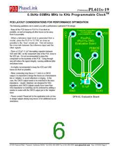
DFN-6L Evaluation Board
47745 Fremont Blvd., Fremont, California 94538 Tel (510) 492-0990 Fax (510) 492-0991 www.phaselink.com Rev 12/12/06 Page 6

 PLL [ PHASELINK CORPORATION ]