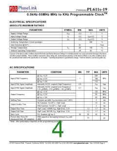
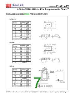
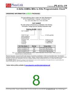
(Preliminary)PL611s-19
0.5kHz-55MHz MHz to KHz Programmable ClockTM
ELECTRICAL SPECIFICATIONS
ABSOLUTE MAXIMUM RATINGS
PARAMETERS
SYMBOL
MIN.
MAX.
UNITS
Supply Voltage Range
VDD
7
V
V
-
-
-
0.5
0.5
0.5
Input Voltage Range
V
VDD
VDD
+
+
0.5
0.5
I
Output Voltage Range
V
V
O
Soldering Temperature (Green package)
Data Retention @ 85°C
260
°C
Year
°C
°C
10
Storage Temperature
-65
-40
150
85
T
S
Ambient Operating Temperature*
Exposure of the device under conditions beyond the limits specified by Maximum Ratings for extended periods may cause permanent damage to the device
and affect product reliability. These conditions represent a stress rating only, and functional operations of the device at these or any other conditions above
the operational limits noted in this specification is not implied. *Operating temperature is guaranteed by design. Parts are tested to commercial grade only.
AC SPECIFICATIONS
PARAMETERS
CONDITIONS
MIN.
TYP.
MAX.
UNITS
@ VDD =3.3V
@ VDD =2.5V
@ VDD =1.8V
200
166
133
VDD
Input (FIN) Frequency
1
MHz
Vpp
Input (FIN) Signal Amplitude
Input (FIN) Signal Amplitude
Internally AC/DC coupled (High Frequency)
Internally AC/DC coupled (Low Frequency)
3.3V <50MHz, 2.5V <40MHz, 1.8V <15MHz
0.9
0.1
VDD
Vpp
@ VDD =3.3V
125
90
65
2
MHz
MHz
MHz
ms
ns
Output Frequency
@ VDD =2.5V
@ VDD =1.8V
Settling Time
At power-up (after VDD increases over 1.62V)
OE Function; Ta=25º C, 15pF Load
PDB Function; Ta=25º C, 15pF Load
15pF Load, 10/90% VDD, High Drive, 3.3V
15pF Load, 90/10% VDD, High Drive, 3.3V
PLL Enabled, @ VDD /2
10
2
Output Enable Time
ms
ns
Output Rise Time
Output Fall Time
Duty Cycle
1.2
1.2
50
1.7
1.7
55
ns
45
%
Period Jitter,Pk-to-Pk*
(measured from 10K samples)
With capacitive decoupling between VDD and
GND.
70
ps
* Note: Jitter performance depends on the programming parameters.
47745 Fremont Blvd., Fremont, California 94538 Tel (510) 492-0990 Fax (510) 492-0991 www.phaselink.com Rev 12/12/06 Page 4

 PLL [ PHASELINK CORPORATION ]