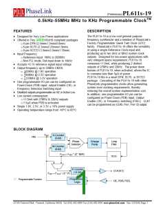
(Preliminary)PL611s-19
0.5kHz-55MHz MHz to KHz Programmable ClockTM
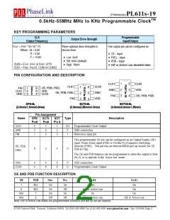
KEY PROGRAMMING PARAMETERS
CLK
Programmable
Input/Output
Output Drive Strength
Output Frequency
F
OUT = FREF * M / (R * P)
Three optional drive strengths to
choose from:
One output pin can be configured as:
Where M = 8 bit
R = 5 bit
• OE - input
• FSEL - input
• PDB – input
P = 14 bit
• Low: 4mA
• Std: 8mA (default)
• High: 16mA
CLK0 = FOUT, FREF or FREF / (2*P)
CLK1 = FREF, FREF/2, CLK0 or CLK0/2
•
HiZ or Active Low disabled state
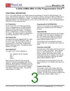
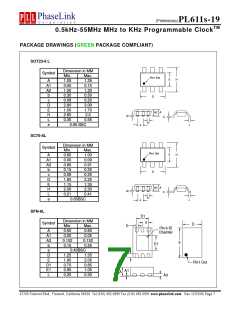
PIN CONFIGURATION AND DESCRIPTION
CLK1
GND
FIN
CLK0
1
2
3
6
5
4
CLK1
CLK0
GND
VDD
1
2
3
6
5
4
OE, PDB, FSEL
VDD
FIN
CLK1
GND
1
2
3
6
5
4
VDD
OE, PDB, FSEL
CLK0
OE, PDB, FSEL
FIN
DFN-6L
(2.0mmx1.3mmx0.6mm)
SC70-6L
(2.3mmx2.25mmx1.0mm)
SOT23-6L
(3.0mmx3.0mmx1.35mm)
Pin Assignment
Name
Type
Description
DFN
Pin#
SC70
Pin#
SOT
Pin #
CLK1
2
3
1
1
5
3
1
2
3
I/O
P
Programmable Clock Output
GND connection
GND
FIN
I
Reference input pin
This programmable I/O pin can be configured as an Output Enable (OE)
input, Power Down input (PDB) or On-the-Fly Frequency Switching
Selector (FSEL). This pin has an internal 60KΩ pull up resistor for OE,
PDB & FSEL.
OE, PDB,
FSEL
6
2
4
O
The OE and PDB features can be programmed to allow the output to float
(Hi Z), or to operate in the ‘Active low’ mode.
VDD
5
4
4
6
5
6
P
VDD connection
CLK0
O
Programmable Clock Output
OE AND PDB FUNCTION DESCRIPTION
OE
PDB
Osc.
PLL
CLK0
CLK1
1
N/A
N/A
1
On
On
On
Off
On
Off
On
Off
On
On
0
HiZ or Active Low
On
On
On
N/A
N/A
0
HiZ or Active Low
HiZ or Active Low
Note: HiZ or Active Low states are programmable functions and will be set per request.
47745 Fremont Blvd., Fremont, California 94538 Tel (510) 492-0990 Fax (510) 492-0991 www.phaselink.com Rev 12/12/06 Page 2

 PLL [ PHASELINK CORPORATION ]