Philips Semiconductors
Preliminary specification
Economy audio CODEC for MiniDisc (MD)
home stereo and portable applications
UDA1341TS
6
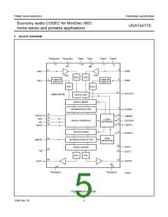
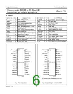
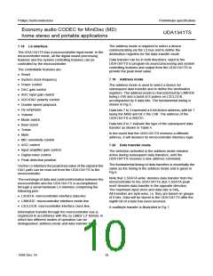
PINNING
SYMBOL
SYMBOL
PIN
DESCRIPTION
PIN
DESCRIPTION
ADC analog ground
L3DATA
BCK
15
16
17
18
19
20
21
22
23
24
25
26
27
28
L3-bus data input and output
bit clock input
VSSA(ADC)
VINL1
1
2
ADC1 input left
WS
word select input
VDDA(ADC)
VINR1
3
ADC analog supply voltage
ADC1 input right
DATAO
DATAI
data output
4
data input
VADCN
5
ADC negative reference voltage
ADC2 input left
TEST1
TEST2
AGCSTAT
QMUTE
VOUTR
VDDA(DAC)
VOUTL
VSSA(DAC)
Vref
test control 1 (pull-down)
test control 2 (pull-down)
AGC status
VINL2
6
VADCP
7
ADC positive reference voltage
ADC2 input right
VINR2
8
quick mute input
OVERFL
VDDD
9
decimation filter overflow output
digital supply voltage
digital ground
DAC output right
10
11
12
13
14
DAC analog supply voltage
DAC output left
VSSD
SYSCLK
L3MODE
L3CLOCK
system clock 256fs, 384fs or 512fs
L3-bus mode input
DAC analog ground
ADC and DAC reference voltage
L3-bus clock input
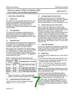
handbook, halfpage
V
handbook, halfpage
V
V
V
1
2
1
2
28
ref
28
ref
SSA(ADC)
VINL1
SSA(ADC)
VINL1
V
V
27
27
SSA(DAC)
SSA(DAC)
V
V
3
VOUTL
3
VOUTL
26
25
24
26
25
24
DDA(ADC)
VINR1
DDA(ADC)
VINR1
V
V
4
4
DDA(DAC)
DDA(DAC)
V
V
VOUTR
VOUTR
5
5
ADCN
ADCN
VINL2
6
23 QMUTE
AGCSTAT
VINL2
6
23 QMUTE
AGCSTAT
V
V
22
7
22
7
ADCP
ADCP
UDA1341TS
UDA1341TS
VINR2
8
21 TEST2
VINR2
8
21 TEST2
OVERFL
TEST1
DATAI
DATAO
WS
OVERFL
TEST1
DATAI
DATAO
WS
9
20
19
18
17
16
9
20
19
18
17
16
V
V
10
11
12
13
10
11
12
13
DDD
DDD
V
V
SSD
SSD
SYSCLK
L3MODE
SYSCLK
L3MODE
BCK
BCK
L3CLOCK 14
15 L3DATA
L3CLOCK 14
15 L3DATA
MGR429
MGR428
Marked pins are compatible with UDA1340M
Fig.2 Pin configuration.
Fig.3 Compatible pins with UDA1340M.
1998 Dec 18
6

 NXP [ NXP ]